SPRS584Q April   2009  – January 2024 TMS320F28030 , TMS320F28030-Q1 , TMS320F28031 , TMS320F28031-Q1 , TMS320F28032 , TMS320F28032-Q1 , TMS320F28033 , TMS320F28033-Q1 , TMS320F28034 , TMS320F28034-Q1 , TMS320F28035 , TMS320F28035-Q1

PRODUCTION DATA  

  1.   1
  2. Features
  3. Applications
  4. Description
    1. 3.1 Functional Block Diagram
  5. Device Comparison
    1. 4.1 Related Products
  6. Pin Configuration and Functions
    1. 5.1 Pin Diagrams
    2. 5.2 Signal Descriptions
  7. Specifications
    1. 6.1  Absolute Maximum Ratings
    2. 6.2  ESD Ratings – Automotive
    3. 6.3  ESD Ratings – Commercial
    4. 6.4  Recommended Operating Conditions
    5. 6.5  Power Consumption Summary
      1. 6.5.1 TMS320F2803x Current Consumption at 60-MHz SYSCLKOUT
      2. 6.5.2 Reducing Current Consumption
      3. 6.5.3 Current Consumption Graphs (VREG Enabled)
    6. 6.6  Electrical Characteristics
    7. 6.7  Thermal Resistance Characteristics
      1. 6.7.1 PN Package
      2. 6.7.2 PAG Package
      3. 6.7.3 RSH Package
    8. 6.8  Thermal Design Considerations
    9. 6.9  JTAG Debug Probe Connection Without Signal Buffering for the MCU
    10. 6.10 Parameter Information
      1. 6.10.1 Timing Parameter Symbology
      2. 6.10.2 General Notes on Timing Parameters
    11. 6.11 Test Load Circuit
    12. 6.12 Power Sequencing
      1. 6.12.1 Reset ( XRS) Timing Requirements
      2. 6.12.2 Reset ( XRS) Switching Characteristics
    13. 6.13 Clock Specifications
      1. 6.13.1 Device Clock Table
        1. 6.13.1.1 2803x Clock Table and Nomenclature (60-MHz Devices)
        2. 6.13.1.2 Device Clocking Requirements/Characteristics
        3. 6.13.1.3 Internal Zero-Pin Oscillator (INTOSC1/INTOSC2) Characteristics
      2. 6.13.2 Clock Requirements and Characteristics
        1. 6.13.2.1 XCLKIN Timing Requirements – PLL Enabled
        2. 6.13.2.2 XCLKIN Timing Requirements – PLL Disabled
        3. 6.13.2.3 XCLKOUT Switching Characteristics (PLL Bypassed or Enabled)
    14. 6.14 Flash Timing
      1. 6.14.1 Flash/OTP Endurance for T Temperature Material
      2. 6.14.2 Flash/OTP Endurance for S Temperature Material
      3. 6.14.3 Flash/OTP Endurance for Q Temperature Material
      4. 6.14.4 Flash Parameters at 60-MHz SYSCLKOUT
      5. 6.14.5 Flash/OTP Access Timing
      6. 6.14.6 Flash Data Retention Duration
  8. Detailed Description
    1. 7.1 Overview
      1. 7.1.1  CPU
      2. 7.1.2  Control Law Accelerator (CLA)
      3. 7.1.3  Memory Bus (Harvard Bus Architecture)
      4. 7.1.4  Peripheral Bus
      5. 7.1.5  Real-Time JTAG and Analysis
      6. 7.1.6  Flash
      7. 7.1.7  M0, M1 SARAMs
      8. 7.1.8  L0 SARAM, and L1, L2, and L3 DPSARAMs
      9. 7.1.9  Boot ROM
        1. 7.1.9.1 Emulation Boot
        2. 7.1.9.2 GetMode
        3. 7.1.9.3 Peripheral Pins Used by the Bootloader
      10. 7.1.10 Security
      11. 7.1.11 Peripheral Interrupt Expansion (PIE) Block
      12. 7.1.12 External Interrupts (XINT1–XINT3)
      13. 7.1.13 Internal Zero Pin Oscillators, Oscillator, and PLL
      14. 7.1.14 Watchdog
      15. 7.1.15 Peripheral Clocking
      16. 7.1.16 Low-power Modes
      17. 7.1.17 Peripheral Frames 0, 1, 2, 3 (PFn)
      18. 7.1.18 General-Purpose Input/Output (GPIO) Multiplexer
      19. 7.1.19 32-Bit CPU-Timers (0, 1, 2)
      20. 7.1.20 Control Peripherals
      21. 7.1.21 Serial Port Peripherals
    2. 7.2 Memory Maps
    3. 7.3 Register Maps
    4. 7.4 Device Emulation Registers
    5. 7.5 VREG/BOR/POR
      1. 7.5.1 On-chip Voltage Regulator (VREG)
        1. 7.5.1.1 Using the On-chip VREG
        2. 7.5.1.2 Disabling the On-chip VREG
      2. 7.5.2 On-chip Power-On Reset (POR) and Brown-Out Reset (BOR) Circuit
    6. 7.6 System Control
      1. 7.6.1 Internal Zero Pin Oscillators
      2. 7.6.2 Crystal Oscillator Option
      3. 7.6.3 PLL-Based Clock Module
      4. 7.6.4 Loss of Input Clock (NMI Watchdog Function)
      5. 7.6.5 CPU Watchdog Module
    7. 7.7 Low-power Modes Block
    8. 7.8 Interrupts
      1. 7.8.1 External Interrupts
        1. 7.8.1.1 External Interrupt Electrical Data/Timing
          1. 7.8.1.1.1 External Interrupt Timing Requirements
          2. 7.8.1.1.2 External Interrupt Switching Characteristics
    9. 7.9 Peripherals
      1. 7.9.1  Control Law Accelerator (CLA) Overview
      2. 7.9.2  Analog Block
        1. 7.9.2.1 Analog-to-Digital Converter (ADC)
          1. 7.9.2.1.1 Features
          2. 7.9.2.1.2 ADC Start-of-Conversion Electrical Data/Timing
            1. 7.9.2.1.2.1 External ADC Start-of-Conversion Switching Characteristics
          3. 7.9.2.1.3 On-Chip Analog-to-Digital Converter (ADC) Electrical Data/Timing
            1. 7.9.2.1.3.1 ADC Electrical Characteristics
            2. 7.9.2.1.3.2 ADC Power Modes
            3. 7.9.2.1.3.3 Internal Temperature Sensor
              1. 7.9.2.1.3.3.1 Temperature Sensor Coefficient
            4. 7.9.2.1.3.4 ADC Power-Up Control Bit Timing
              1. 7.9.2.1.3.4.1 ADC Power-Up Delays
            5. 7.9.2.1.3.5 ADC Sequential and Simultaneous Timings
        2. 7.9.2.2 ADC MUX
        3. 7.9.2.3 Comparator Block
          1. 7.9.2.3.1 On-Chip Comparator/DAC Electrical Data/Timing
            1. 7.9.2.3.1.1 Electrical Characteristics of the Comparator/DAC
      3. 7.9.3  Detailed Descriptions
      4. 7.9.4  Serial Peripheral Interface (SPI) Module
        1. 7.9.4.1 SPI Master Mode Electrical Data/Timing
          1. 7.9.4.1.1 SPI Master Mode External Timing (Clock Phase = 0)
          2. 7.9.4.1.2 SPI Master Mode External Timing (Clock Phase = 1)
        2. 7.9.4.2 SPI Slave Mode Electrical Data/Timing
          1. 7.9.4.2.1 SPI Slave Mode External Timing (Clock Phase = 0)
          2. 7.9.4.2.2 SPI Slave Mode External Timing (Clock Phase = 1)
      5. 7.9.5  Serial Communications Interface (SCI) Module
      6. 7.9.6  Local Interconnect Network (LIN)
      7. 7.9.7  Enhanced Controller Area Network (eCAN) Module
      8. 7.9.8  Inter-Integrated Circuit (I2C)
        1. 7.9.8.1 I2C Electrical Data/Timing
          1. 7.9.8.1.1 I2C Timing Requirements
          2. 7.9.8.1.2 I2C Switching Characteristics
      9. 7.9.9  Enhanced PWM Modules (ePWM1/2/3/4/5/6/7)
        1. 7.9.9.1 ePWM Electrical Data/Timing
          1. 7.9.9.1.1 ePWM Timing Requirements
          2. 7.9.9.1.2 ePWM Switching Characteristics
        2. 7.9.9.2 Trip-Zone Input Timing
          1. 7.9.9.2.1 Trip-Zone Input Timing Requirements
      10. 7.9.10 High-Resolution PWM (HRPWM)
        1. 7.9.10.1 HRPWM Electrical Data/Timing
          1. 7.9.10.1.1 High-Resolution PWM Characteristics
      11. 7.9.11 Enhanced Capture Module (eCAP1)
        1. 7.9.11.1 eCAP Electrical Data/Timing
          1. 7.9.11.1.1 Enhanced Capture (eCAP) Timing Requirement
          2. 7.9.11.1.2 eCAP Switching Characteristics
      12. 7.9.12 High-Resolution Capture (HRCAP) Module
        1. 7.9.12.1 HRCAP Electrical Data/Timing
          1. 7.9.12.1.1 High-Resolution Capture (HRCAP) Timing Requirements
      13. 7.9.13 Enhanced Quadrature Encoder Pulse (eQEP)
        1. 7.9.13.1 eQEP Electrical Data/Timing
          1. 7.9.13.1.1 Enhanced Quadrature Encoder Pulse (eQEP) Timing Requirements
          2. 7.9.13.1.2 eQEP Switching Characteristics
      14. 7.9.14 JTAG Port
      15. 7.9.15 General-Purpose Input/Output (GPIO) MUX
        1. 7.9.15.1 GPIO Electrical Data/Timing
          1. 7.9.15.1.1 GPIO - Output Timing
            1. 7.9.15.1.1.1 General-Purpose Output Switching Characteristics
          2. 7.9.15.1.2 GPIO - Input Timing
            1. 7.9.15.1.2.1 General-Purpose Input Timing Requirements
          3. 7.9.15.1.3 Sampling Window Width for Input Signals
          4. 7.9.15.1.4 Low-Power Mode Wakeup Timing
            1. 7.9.15.1.4.1 IDLE Mode Timing Requirements
            2. 7.9.15.1.4.2 IDLE Mode Switching Characteristics
            3. 7.9.15.1.4.3 STANDBY Mode Timing Requirements
            4. 7.9.15.1.4.4 STANDBY Mode Switching Characteristics
            5. 7.9.15.1.4.5 HALT Mode Timing Requirements
            6. 7.9.15.1.4.6 HALT Mode Switching Characteristics
  9. Applications, Implementation, and Layout
    1. 8.1 TI Reference Design
  10. Device and Documentation Support
    1. 9.1 Device and Development Support Tool Nomenclature
    2. 9.2 Tools and Software
    3. 9.3 Documentation Support
    4. 9.4 Support Resources
    5. 9.5 Trademarks
    6. 9.6 Electrostatic Discharge Caution
    7. 9.7 Glossary
  11. 10Revision History
  12. 11Mechanical, Packaging, and Orderable Information
    1. 11.1 Packaging Information

Package Options

Mechanical Data (Package|Pins)
Thermal pad, mechanical data (Package|Pins)
Orderable Information

Inter-Integrated Circuit (I2C)

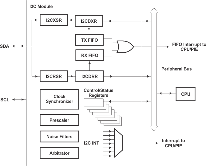
The device contains one I2C Serial Port. Figure 7-37 shows how the I2C peripheral module interfaces within the device.

The I2C module has the following features:

  • Compliance with the Philips Semiconductors I2C-bus specification (version 2.1):
    • Support for 1-bit to 8-bit format transfers
    • 7-bit and 10-bit addressing modes
    • General call
    • START byte mode
    • Support for multiple master-transmitters and slave-receivers
    • Support for multiple slave-transmitters and master-receivers
    • Combined master transmit/receive and receive/transmit mode
    • Data transfer rate of from 10 kbps up to 400 kbps (I2C Fast-mode rate)
  • One 4-word receive FIFO and one 4-word transmit FIFO
  • One interrupt that can be used by the CPU. This interrupt can be generated as a result of one of the following conditions:
    • Transmit-data ready
    • Receive-data ready
    • Register-access ready
    • No-acknowledgment received
    • Arbitration lost
    • Stop condition detected
    • Addressed as slave
  • An additional interrupt that can be used by the CPU when in FIFO mode
  • Module enable/disable capability
  • Free data format mode

For more information on the I2C, see the Inter-Integrated Circuit Module (I2C) chapter in the TMS320F2803x Real-Time Microcontrollers Technical Reference Manual.
GUID-ABCBCB72-5B67-444D-A545-F0798A7FC725-low.gif
The I2C registers are accessed at the SYSCLKOUT rate. The internal timing and signal waveforms of the I2C port are also at the SYSCLKOUT rate.
The clock enable bit (I2CAENCLK) in the PCLKCRO register turns off the clock to the I2C port for low-power operation. Upon reset, I2CAENCLK is clear, which indicates the peripheral internal clocks are off.
Figure 7-37 I2C Peripheral Module Interfaces

The registers in Table 7-33 configure and control the I2C port operation.

Table 7-33 I2C-A Registers
NAMEADDRESSEALLOW PROTECTEDDESCRIPTION
I2COAR0x7900NoI2C own address register
I2CIER0x7901NoI2C interrupt enable register
I2CSTR0x7902NoI2C status register
I2CCLKL0x7903NoI2C clock low-time divider register
I2CCLKH0x7904NoI2C clock high-time divider register
I2CCNT0x7905NoI2C data count register
I2CDRR0x7906NoI2C data receive register
I2CSAR0x7907NoI2C slave address register
I2CDXR0x7908NoI2C data transmit register
I2CMDR0x7909NoI2C mode register
I2CISRC0x790ANoI2C interrupt source register
I2CPSC0x790CNoI2C prescaler register
I2CFFTX0x7920NoI2C FIFO transmit register
I2CFFRX0x7921NoI2C FIFO receive register
I2CRSRNoI2C receive shift register (not accessible to the CPU)
I2CXSRNoI2C transmit shift register (not accessible to the CPU)