SPRS584Q April   2009  – January 2024 TMS320F28030 , TMS320F28030-Q1 , TMS320F28031 , TMS320F28031-Q1 , TMS320F28032 , TMS320F28032-Q1 , TMS320F28033 , TMS320F28033-Q1 , TMS320F28034 , TMS320F28034-Q1 , TMS320F28035 , TMS320F28035-Q1

PRODUCTION DATA  

  1.   1
  2. Features
  3. Applications
  4. Description
    1. 3.1 Functional Block Diagram
  5. Device Comparison
    1. 4.1 Related Products
  6. Pin Configuration and Functions
    1. 5.1 Pin Diagrams
    2. 5.2 Signal Descriptions
  7. Specifications
    1. 6.1  Absolute Maximum Ratings
    2. 6.2  ESD Ratings – Automotive
    3. 6.3  ESD Ratings – Commercial
    4. 6.4  Recommended Operating Conditions
    5. 6.5  Power Consumption Summary
      1. 6.5.1 TMS320F2803x Current Consumption at 60-MHz SYSCLKOUT
      2. 6.5.2 Reducing Current Consumption
      3. 6.5.3 Current Consumption Graphs (VREG Enabled)
    6. 6.6  Electrical Characteristics
    7. 6.7  Thermal Resistance Characteristics
      1. 6.7.1 PN Package
      2. 6.7.2 PAG Package
      3. 6.7.3 RSH Package
    8. 6.8  Thermal Design Considerations
    9. 6.9  JTAG Debug Probe Connection Without Signal Buffering for the MCU
    10. 6.10 Parameter Information
      1. 6.10.1 Timing Parameter Symbology
      2. 6.10.2 General Notes on Timing Parameters
    11. 6.11 Test Load Circuit
    12. 6.12 Power Sequencing
      1. 6.12.1 Reset ( XRS) Timing Requirements
      2. 6.12.2 Reset ( XRS) Switching Characteristics
    13. 6.13 Clock Specifications
      1. 6.13.1 Device Clock Table
        1. 6.13.1.1 2803x Clock Table and Nomenclature (60-MHz Devices)
        2. 6.13.1.2 Device Clocking Requirements/Characteristics
        3. 6.13.1.3 Internal Zero-Pin Oscillator (INTOSC1/INTOSC2) Characteristics
      2. 6.13.2 Clock Requirements and Characteristics
        1. 6.13.2.1 XCLKIN Timing Requirements – PLL Enabled
        2. 6.13.2.2 XCLKIN Timing Requirements – PLL Disabled
        3. 6.13.2.3 XCLKOUT Switching Characteristics (PLL Bypassed or Enabled)
    14. 6.14 Flash Timing
      1. 6.14.1 Flash/OTP Endurance for T Temperature Material
      2. 6.14.2 Flash/OTP Endurance for S Temperature Material
      3. 6.14.3 Flash/OTP Endurance for Q Temperature Material
      4. 6.14.4 Flash Parameters at 60-MHz SYSCLKOUT
      5. 6.14.5 Flash/OTP Access Timing
      6. 6.14.6 Flash Data Retention Duration
  8. Detailed Description
    1. 7.1 Overview
      1. 7.1.1  CPU
      2. 7.1.2  Control Law Accelerator (CLA)
      3. 7.1.3  Memory Bus (Harvard Bus Architecture)
      4. 7.1.4  Peripheral Bus
      5. 7.1.5  Real-Time JTAG and Analysis
      6. 7.1.6  Flash
      7. 7.1.7  M0, M1 SARAMs
      8. 7.1.8  L0 SARAM, and L1, L2, and L3 DPSARAMs
      9. 7.1.9  Boot ROM
        1. 7.1.9.1 Emulation Boot
        2. 7.1.9.2 GetMode
        3. 7.1.9.3 Peripheral Pins Used by the Bootloader
      10. 7.1.10 Security
      11. 7.1.11 Peripheral Interrupt Expansion (PIE) Block
      12. 7.1.12 External Interrupts (XINT1–XINT3)
      13. 7.1.13 Internal Zero Pin Oscillators, Oscillator, and PLL
      14. 7.1.14 Watchdog
      15. 7.1.15 Peripheral Clocking
      16. 7.1.16 Low-power Modes
      17. 7.1.17 Peripheral Frames 0, 1, 2, 3 (PFn)
      18. 7.1.18 General-Purpose Input/Output (GPIO) Multiplexer
      19. 7.1.19 32-Bit CPU-Timers (0, 1, 2)
      20. 7.1.20 Control Peripherals
      21. 7.1.21 Serial Port Peripherals
    2. 7.2 Memory Maps
    3. 7.3 Register Maps
    4. 7.4 Device Emulation Registers
    5. 7.5 VREG/BOR/POR
      1. 7.5.1 On-chip Voltage Regulator (VREG)
        1. 7.5.1.1 Using the On-chip VREG
        2. 7.5.1.2 Disabling the On-chip VREG
      2. 7.5.2 On-chip Power-On Reset (POR) and Brown-Out Reset (BOR) Circuit
    6. 7.6 System Control
      1. 7.6.1 Internal Zero Pin Oscillators
      2. 7.6.2 Crystal Oscillator Option
      3. 7.6.3 PLL-Based Clock Module
      4. 7.6.4 Loss of Input Clock (NMI Watchdog Function)
      5. 7.6.5 CPU Watchdog Module
    7. 7.7 Low-power Modes Block
    8. 7.8 Interrupts
      1. 7.8.1 External Interrupts
        1. 7.8.1.1 External Interrupt Electrical Data/Timing
          1. 7.8.1.1.1 External Interrupt Timing Requirements
          2. 7.8.1.1.2 External Interrupt Switching Characteristics
    9. 7.9 Peripherals
      1. 7.9.1  Control Law Accelerator (CLA) Overview
      2. 7.9.2  Analog Block
        1. 7.9.2.1 Analog-to-Digital Converter (ADC)
          1. 7.9.2.1.1 Features
          2. 7.9.2.1.2 ADC Start-of-Conversion Electrical Data/Timing
            1. 7.9.2.1.2.1 External ADC Start-of-Conversion Switching Characteristics
          3. 7.9.2.1.3 On-Chip Analog-to-Digital Converter (ADC) Electrical Data/Timing
            1. 7.9.2.1.3.1 ADC Electrical Characteristics
            2. 7.9.2.1.3.2 ADC Power Modes
            3. 7.9.2.1.3.3 Internal Temperature Sensor
              1. 7.9.2.1.3.3.1 Temperature Sensor Coefficient
            4. 7.9.2.1.3.4 ADC Power-Up Control Bit Timing
              1. 7.9.2.1.3.4.1 ADC Power-Up Delays
            5. 7.9.2.1.3.5 ADC Sequential and Simultaneous Timings
        2. 7.9.2.2 ADC MUX
        3. 7.9.2.3 Comparator Block
          1. 7.9.2.3.1 On-Chip Comparator/DAC Electrical Data/Timing
            1. 7.9.2.3.1.1 Electrical Characteristics of the Comparator/DAC
      3. 7.9.3  Detailed Descriptions
      4. 7.9.4  Serial Peripheral Interface (SPI) Module
        1. 7.9.4.1 SPI Master Mode Electrical Data/Timing
          1. 7.9.4.1.1 SPI Master Mode External Timing (Clock Phase = 0)
          2. 7.9.4.1.2 SPI Master Mode External Timing (Clock Phase = 1)
        2. 7.9.4.2 SPI Slave Mode Electrical Data/Timing
          1. 7.9.4.2.1 SPI Slave Mode External Timing (Clock Phase = 0)
          2. 7.9.4.2.2 SPI Slave Mode External Timing (Clock Phase = 1)
      5. 7.9.5  Serial Communications Interface (SCI) Module
      6. 7.9.6  Local Interconnect Network (LIN)
      7. 7.9.7  Enhanced Controller Area Network (eCAN) Module
      8. 7.9.8  Inter-Integrated Circuit (I2C)
        1. 7.9.8.1 I2C Electrical Data/Timing
          1. 7.9.8.1.1 I2C Timing Requirements
          2. 7.9.8.1.2 I2C Switching Characteristics
      9. 7.9.9  Enhanced PWM Modules (ePWM1/2/3/4/5/6/7)
        1. 7.9.9.1 ePWM Electrical Data/Timing
          1. 7.9.9.1.1 ePWM Timing Requirements
          2. 7.9.9.1.2 ePWM Switching Characteristics
        2. 7.9.9.2 Trip-Zone Input Timing
          1. 7.9.9.2.1 Trip-Zone Input Timing Requirements
      10. 7.9.10 High-Resolution PWM (HRPWM)
        1. 7.9.10.1 HRPWM Electrical Data/Timing
          1. 7.9.10.1.1 High-Resolution PWM Characteristics
      11. 7.9.11 Enhanced Capture Module (eCAP1)
        1. 7.9.11.1 eCAP Electrical Data/Timing
          1. 7.9.11.1.1 Enhanced Capture (eCAP) Timing Requirement
          2. 7.9.11.1.2 eCAP Switching Characteristics
      12. 7.9.12 High-Resolution Capture (HRCAP) Module
        1. 7.9.12.1 HRCAP Electrical Data/Timing
          1. 7.9.12.1.1 High-Resolution Capture (HRCAP) Timing Requirements
      13. 7.9.13 Enhanced Quadrature Encoder Pulse (eQEP)
        1. 7.9.13.1 eQEP Electrical Data/Timing
          1. 7.9.13.1.1 Enhanced Quadrature Encoder Pulse (eQEP) Timing Requirements
          2. 7.9.13.1.2 eQEP Switching Characteristics
      14. 7.9.14 JTAG Port
      15. 7.9.15 General-Purpose Input/Output (GPIO) MUX
        1. 7.9.15.1 GPIO Electrical Data/Timing
          1. 7.9.15.1.1 GPIO - Output Timing
            1. 7.9.15.1.1.1 General-Purpose Output Switching Characteristics
          2. 7.9.15.1.2 GPIO - Input Timing
            1. 7.9.15.1.2.1 General-Purpose Input Timing Requirements
          3. 7.9.15.1.3 Sampling Window Width for Input Signals
          4. 7.9.15.1.4 Low-Power Mode Wakeup Timing
            1. 7.9.15.1.4.1 IDLE Mode Timing Requirements
            2. 7.9.15.1.4.2 IDLE Mode Switching Characteristics
            3. 7.9.15.1.4.3 STANDBY Mode Timing Requirements
            4. 7.9.15.1.4.4 STANDBY Mode Switching Characteristics
            5. 7.9.15.1.4.5 HALT Mode Timing Requirements
            6. 7.9.15.1.4.6 HALT Mode Switching Characteristics
  9. Applications, Implementation, and Layout
    1. 8.1 TI Reference Design
  10. Device and Documentation Support
    1. 9.1 Device and Development Support Tool Nomenclature
    2. 9.2 Tools and Software
    3. 9.3 Documentation Support
    4. 9.4 Support Resources
    5. 9.5 Trademarks
    6. 9.6 Electrostatic Discharge Caution
    7. 9.7 Glossary
  11. 10Revision History
  12. 11Mechanical, Packaging, and Orderable Information
    1. 11.1 Packaging Information

Package Options

Mechanical Data (Package|Pins)
Thermal pad, mechanical data (Package|Pins)
Orderable Information

Enhanced Capture Module (eCAP1)

The device contains an enhanced capture (eCAP) module. Figure 7-41 shows a functional block diagram of a module.
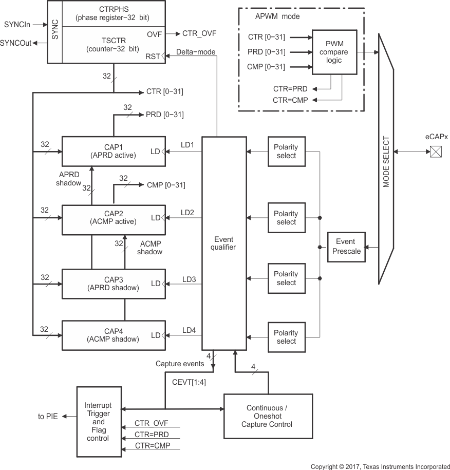
GUID-6316BC99-DDAA-42FF-BB0D-9C9509966E0D-low.gifFigure 7-41 eCAP Functional Block Diagram

The eCAP module is clocked at the SYSCLKOUT rate.

The clock enable bits (ECAP1 ENCLK) in the PCLKCR1 register turn off the eCAP module individually (for low-power operation). Upon reset, ECAP1ENCLK is set to low, indicating that the peripheral clock is off.

Table 7-36 eCAP Control and Status Registers
NAME eCAP1 SIZE (x16) EALLOW PROTECTED DESCRIPTION
TSCTR 0x6A00 2 Time-Stamp Counter
CTRPHS 0x6A02 2 Counter Phase Offset Value Register
CAP1 0x6A04 2 Capture 1 Register
CAP2 0x6A06 2 Capture 2 Register
CAP3 0x6A08 2 Capture 3 Register
CAP4 0x6A0A 2 Capture 4 Register
Reserved 0x6A0C to 0x6A12 8 Reserved
ECCTL1 0x6A14 1 Capture Control Register 1
ECCTL2 0x6A15 1 Capture Control Register 2
ECEINT 0x6A16 1 Capture Interrupt Enable Register
ECFLG 0x6A17 1 Capture Interrupt Flag Register
ECCLR 0x6A18 1 Capture Interrupt Clear Register
ECFRC 0x6A19 1 Capture Interrupt Force Register
Reserved 0x6A1A to 0x6A1F 6 Reserved

For more information on the eCAP, see the Enhanced Capture (eCAP) Module chapter in the TMS320F2803x Real-Time Microcontrollers Technical Reference Manual.