SCDS412B June 2019 – January 2024 TMUX1133 , TMUX1134
PRODUCTION DATA
- 1
- 1 Features
- 2 Applications
- 3 Description
- 4 Device Comparison Table
- 5 Pin Configuration and Functions
-
6 Specifications
- 6.1 Absolute Maximum Ratings
- 6.2 ESD Ratings
- 6.3 Recommended Operating Conditions
- 6.4 Thermal Information
- 6.5 Electrical Characteristics (VDD = 5V ±10 %)
- 6.6 Electrical Characteristics (VDD = 3.3V ±10 %)
- 6.7 Electrical Characteristics (VDD = 2.5V ±10 %), (VSS = –2.5V ±10 %)
- 6.8 Electrical Characteristics (VDD = 1.8V ±10 %)
- 6.9 Electrical Characteristics (VDD = 1.2V ±10 %)
- 6.10 Typical Characteristics
- 7 Parameter Measurement Information
- 8 Detailed Description
- 9 Application and Implementation
- 10Device and Documentation Support
- 11Revision History
- 12Mechanical, Packaging, and Orderable Information
Package Options
Mechanical Data (Package|Pins)
- PW|20
Thermal pad, mechanical data (Package|Pins)
- PW|20
Orderable Information
3 Description
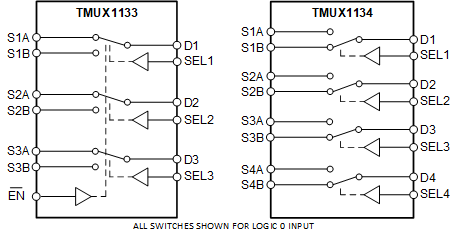
The TMUX113x devices are precision complementary metal-oxide semiconductor (CMOS) switches with multiple channels. The TMUX1133 is a 2:1, single-pole double-throw (SPDT), configuration with three independently controlled channels and an EN pin to enable or disable all three switches. The TMUX1134 contains four independently controlled SPDT switches. Wide operating supply of 1.08V to 5.5V, or ±2.75V dual supply, allows for use in a broad array of applications from medical equipment to industrial systems. The device supports bidirectional analog and digital signals on the source (Sx) and drain (Dx) pins ranging from VSS to VDD. For single supply applications VSS must be connected to GND.
All logic inputs have 1.8V logic compatible thresholds, allowing for both TTL and CMOS logic compatibility when operating in the valid supply voltage range. Fail-Safe Logic circuitry allows voltages on the control pins to be applied before the supply pin, protecting the device from potential damage.
The TMUX113x devices are part of the precision switches and multiplexers family. These devices have very low on and off leakage currents and low charge injection, allowing them to be used in high precision measurement applications. A low supply current of
8nA enables use in portable applications.
| PART NUMBER | CHANNEL COUNT(1) | PACKAGE(2) |
|---|---|---|
| TMUX1133 | 3-Channel | PW (TSSOP, 16) |
| TMUX1134 | 4-Channel | PW (TSSOP, 20) |
 TMUX113x Block Diagrams