SLOS650F August 2009 – June 2016 TPA3113D2
PRODUCTION DATA.
- 1 Features
- 2 Applications
- 3 Description
- 4 Revision History
- 5 Pin Configuration and Functions
-
6 Specifications
- 6.1 Absolute Maximum Ratings
- 6.2 ESD Ratings
- 6.3 Recommended Operating Conditions
- 6.4 Thermal Information
- 6.5 DC Electrical Characteristics, VCC = 24 V
- 6.6 DC Electrical Characteristics, VCC = 12 V
- 6.7 AC Electrical Characteristics, VCC = 24 V
- 6.8 AC Electrical Characteristics, VCC = 12 V
- 6.9 Typical Characteristics
- 7 Detailed Description
-
8 Application and Implementation
- 8.1 Application Information
- 8.2
Typical Applications
- 8.2.1
Stereo Class-D Amplifier With BTL Output
- 8.2.1.1 Design Requirements
- 8.2.1.2
Detailed Design Procedure
- 8.2.1.2.1 Ferrite Bead Filter Considerations
- 8.2.1.2.2 Efficiency: LC Filter Required With the Traditional Class-D Modulation Scheme
- 8.2.1.2.3 When to Use an Output Filter for EMI Suppression
- 8.2.1.2.4 Input Resistance
- 8.2.1.2.5 Input Capacitor, CI
- 8.2.1.2.6 BSN and BSP Capacitors
- 8.2.1.2.7 Differential Inputs
- 8.2.1.2.8 Using LOW-ESR Capacitors
- 8.2.1.3 Application Curves
- 8.2.2 Stereo Class-D Amplifier With BTL Output
- 8.2.3 Stereo Class-D Amplifier With PBTL Output
- 8.2.1
Stereo Class-D Amplifier With BTL Output
- 9 Power Supply Recommendations
- 10Layout
- 11Device and Documentation Support
- 12Mechanical, Packaging, and Orderable Information
Package Options
Mechanical Data (Package|Pins)
- PWP|28
Thermal pad, mechanical data (Package|Pins)
- PWP|28
Orderable Information
6 Specifications
6.1 Absolute Maximum Ratings
over operating free-air temperature range (unless otherwise noted)(1)| MIN | MAX | UNIT | |||
|---|---|---|---|---|---|
| VCC | Supply voltage | AVCC, PVCC | –0.3 | 30 | V |
| VI | Interface pin voltage | SD, GAIN0, GAIN1, PBTL, FAULT (2) | –0.3 | VCC + 0.3 | V |
| < 10 | V/ms | ||||
| PLIMIT | –0.3 | GVDD + 0.3 | V | ||
| RINN, RINP, LINN, LINP | –0.3 | 6.3 | V | ||
| Continuous total power dissipation | See Thermal Information | ||||
| TA | Operating free-air temperature | –40 | 85 | °C | |
| TJ | Operating junction temperature(3) | –40 | 150 | °C | |
| RL | Minimum load resistance | BTL: PVCC > 15 V | 4.8 | Ω | |
| BTL: PVCC ≤ 15 V | 3.2 | ||||
| PBTL | 3.2 | ||||
| Tstg | Storage temperature | –65 | 150 | °C | |
(1) Stresses beyond those listed under Absolute Maximum Ratings may cause permanent damage to the device. These are stress ratings only, which do not imply functional operation of the device at these or any other conditions beyond those indicated under Recommended Operating Conditions. Exposure to absolute-maximum-rated conditions for extended periods may affect device reliability.
(2) The voltage slew rate of these pins must be restricted to no more than 10 V/ms. For higher slew rates, use a 100-kΩ resister in series with the pins.
(3) The TPA3113D2 incorporates an exposed thermal pad on the underside of the chip. This acts as a heatsink, and it must be connected to a thermally dissipating plane for proper power dissipation. Failure to do so may result in the device going into thermal protection shutdown. See TI Technical Briefs Quad Flatpack No-Lead Logic Packages for more information about using the TSSOP thermal pad.
6.2 ESD Ratings
| VALUE | UNIT | |||
|---|---|---|---|---|
| V(ESD) | Electrostatic discharge | Human-body model (HBM), per ANSI/ESDA/JEDEC JS-001(1)(3) | ±2000 | V |
| Charged-device model (CDM), per JEDEC specification JESD22-C101(2)(4) | ±500 | |||
(1) JEDEC document JEP155 states that 500-V HBM allows safe manufacturing with a standard ESD control process.
(2) JEDEC document JEP157 states that 250-V CDM allows safe manufacturing with a standard ESD control process.
(3) In accordance with JEDEC Standard 22, Test Method A114-B.
(4) In accordance with JEDEC Standard 22, Test Method C101-A
6.3 Recommended Operating Conditions
over operating free-air temperature range (unless otherwise noted)| MIN | MAX | UNIT | |||
|---|---|---|---|---|---|
| VCC | Supply voltage | PVCC, AVCC | 8 | 26 | V |
| VIH | High-level input voltage | SD, GAIN0, GAIN1, PBTL | 2 | V | |
| VIL | Low-level input voltage | SD, GAIN0, GAIN1, PBTL | 0.8 | V | |
| VOL | Low-level output voltage | FAULT, RPULLUP = 100k, VCC = 26 V | 0.8 | V | |
| IIH | High-level input current | SD, GAIN0, GAIN1, PBTL, VI = 2 V, VCC = 18 V | 50 | µA | |
| IIL | Low-level input current | SD, GAIN0, GAIN1, PBTL, VI = 0.8 V, VCC = 18 V | 5 | µA | |
| TA | Operating free-air temperature | –40 | 85 | °C | |
6.4 Thermal Information
| THERMAL METRIC(1)(2) | TPA3113D2 | UNIT | |
|---|---|---|---|
| PWP (TSSOP) | |||
| 28 PINS | |||
| RθJA | Junction-to-ambient thermal resistance | 30.3 | °C/W |
| RθJC(top) | Junction-to-case (top) thermal resistance | 33.5 | °C/W |
| RθJB | Junction-to-board thermal resistance | 17.5 | °C/W |
| ψJT | Junction-to-top characterization parameter | 0.9 | °C/W |
| ψJB | Junction-to-board characterization parameter | 7.2 | °C/W |
| RθJC(bot) | Junction-to-case (bottom) thermal resistance | 0.9 | °C/W |
(1) For more information about traditional and new thermal metrics, see the application report Semiconductor and IC Package Thermal Metrics.
(2) For thermal estimates of this device based on PCB copper area, see the PCB Thermal Calculator.
6.5 DC Electrical Characteristics, VCC = 24 V
TA = 25°C, VCC = 24 V, RL = 8 Ω (unless otherwise noted)6.6 DC Electrical Characteristics, VCC = 12 V
TA = 25°C, VCC = 12 V, RL = 8 Ω (unless otherwise noted)6.7 AC Electrical Characteristics, VCC = 24 V
TA = 25°C, VCC = 24 V, RL = 8 Ω (unless otherwise noted)6.8 AC Electrical Characteristics, VCC = 12 V
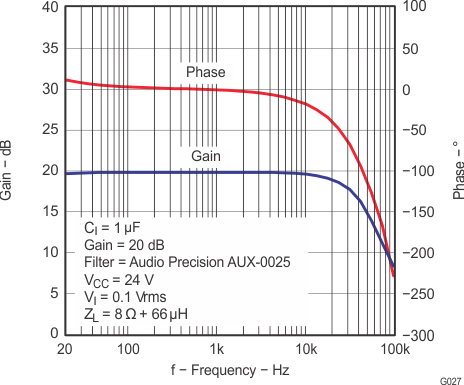
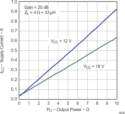
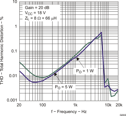
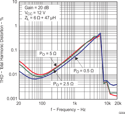
TA = 25°C, VCC = 12 V, RL = 8 Ω (unless otherwise noted)6.9 Typical Characteristics
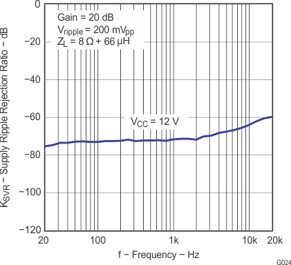
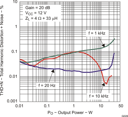
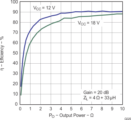
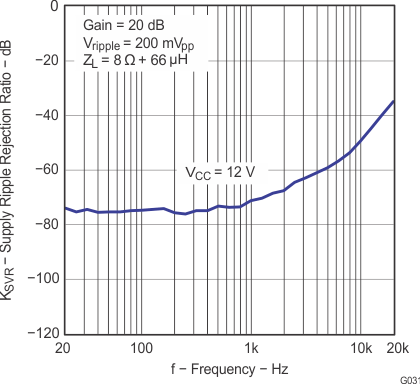
(All Measurements taken at 1 kHz, unless otherwise noted. Measurements were made using the TPA3113D2 EVM which is available at ti.com.)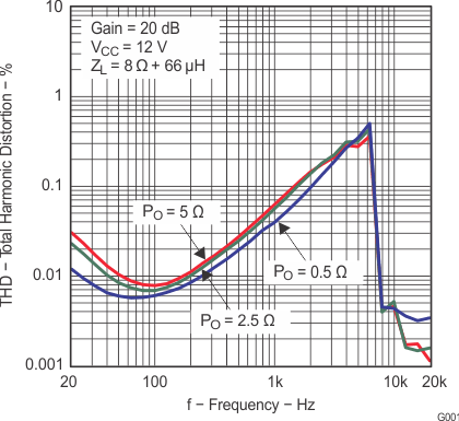
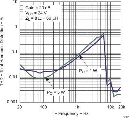
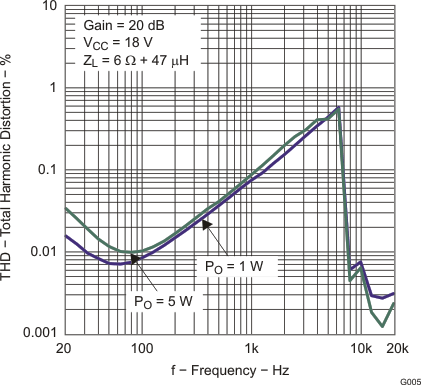
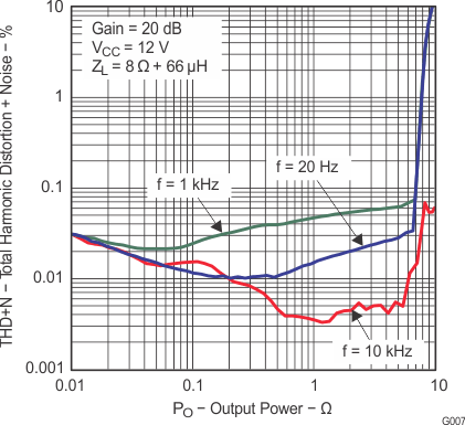
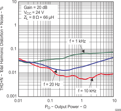
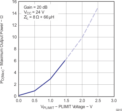
| Dashed line represents thermally limited region. |
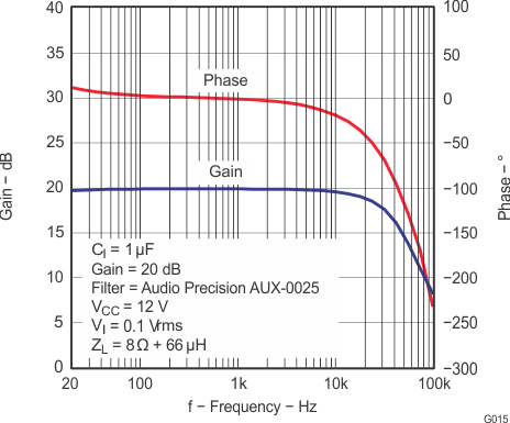
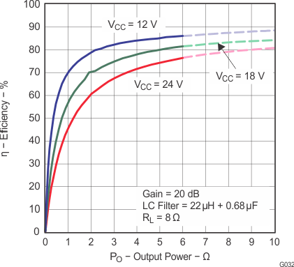
| Dashed lines represent thermally limited region. |
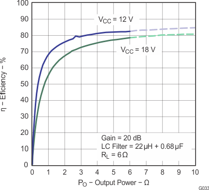
| Dashed lines represent thermally limited region. |
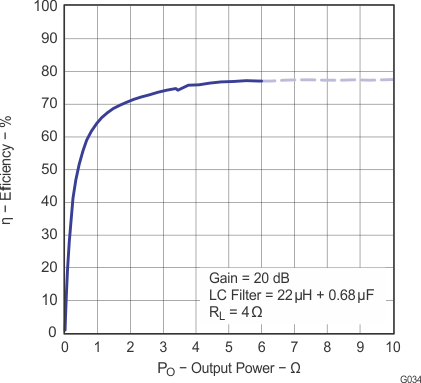
| Dashed lines represent thermally limited region. |
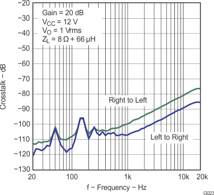
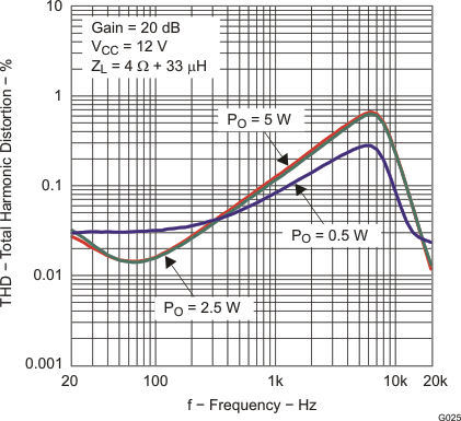
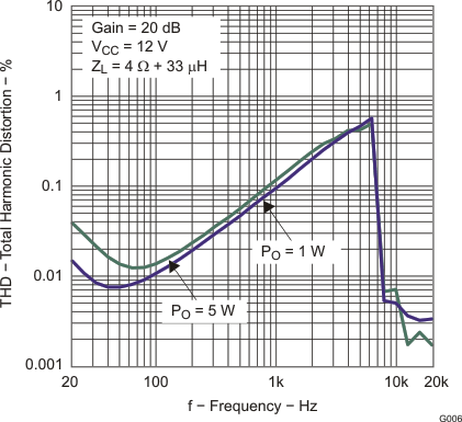
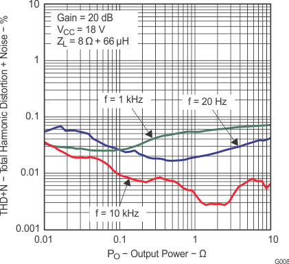
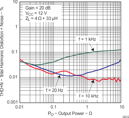
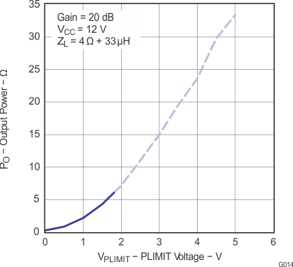
| Dashed line represents thermally limited region. |
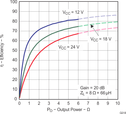
| Dashed lines represent thermally limited region. |
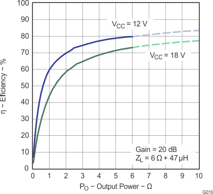
| Dashed lines represent thermally limited region. |
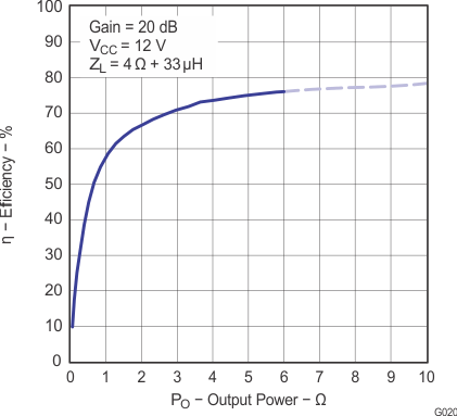
| Dashed lines represent thermally limited region. |
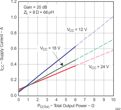
| Dashed lines represent thermally limited region. |
