SLVSC54B July 2013 – April 2014 TPD4E110
PRODUCTION DATA.
- 1 Features
- 2 Applications
- 3 Description
- 4 Simplified Schematic
- 5 Revision History
- 6 Terminal Configuration and Functions
- 7 Specifications
- 8 Detailed Description
- 9 Applications and Implementation
- 10Layout
- 11Device and Documentation Support
- 12Mechanical, Packaging, and Orderable Information
Package Options
Mechanical Data (Package|Pins)
- DPW|4
Thermal pad, mechanical data (Package|Pins)
- DPW|4
Orderable Information
9 Applications and Implementation
9.1 Application Information
TPD4E110 is a diode array type Transient Voltage Suppressor (TVS) which is typically used to provide a path to ground for dissipating ESD events on hi-speed signal lines between a human interface connector and a system. As the current from ESD passes through the TVS, only a small voltage drop is present across the diode. This is the voltage presented to the protected IC. The low RDYN of the triggered TVS holds this voltage, VCLAMP, to a tolerable level to the protected IC.
9.2 Typical Application
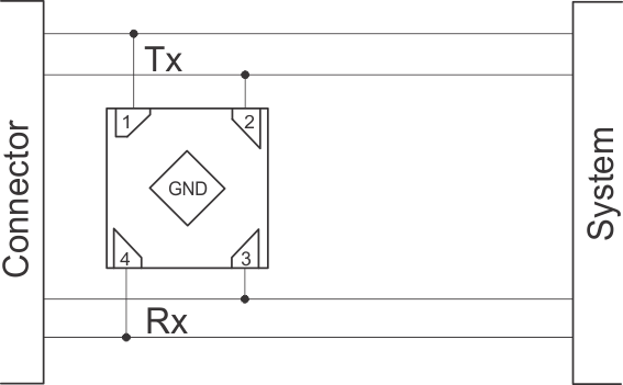 Figure 10. Protecting a Pair of Super-Speed Data Lines
9.2.1 Design Requirements
For this design example, use the following as the input parameters.
Table 1. Design Parameters
| DESIGN PARAMETER | EXAMPLE VALUE |
|---|---|
| Signal range on Pin 1, 2, 3, or 4 | 0V to 5.5V |
| Operating Frequency | 3.0 GHz |
9.2.2 Detailed Design Procedure
To begin the design process some parameters must be decided upon. The designer needs to know the following:
- Signal range on all the protected lines
- Operating frequency
9.2.2.1 Signal range on Terminal 1, 2, 3, or 4
TPD4E110 has 4 identical protection channels for signal lines. The symmetry of TPD4E110 provides flexibility when selecting which of the 4 IO channels will protect which signal lines. Any IO will support a signal range of 0V to 5.5V.
9.2.2.2 Operating Frequency
The 0.45pF capacitance of each IO channel supports data rates up to 6Gbps.
9.2.3 Application Curves
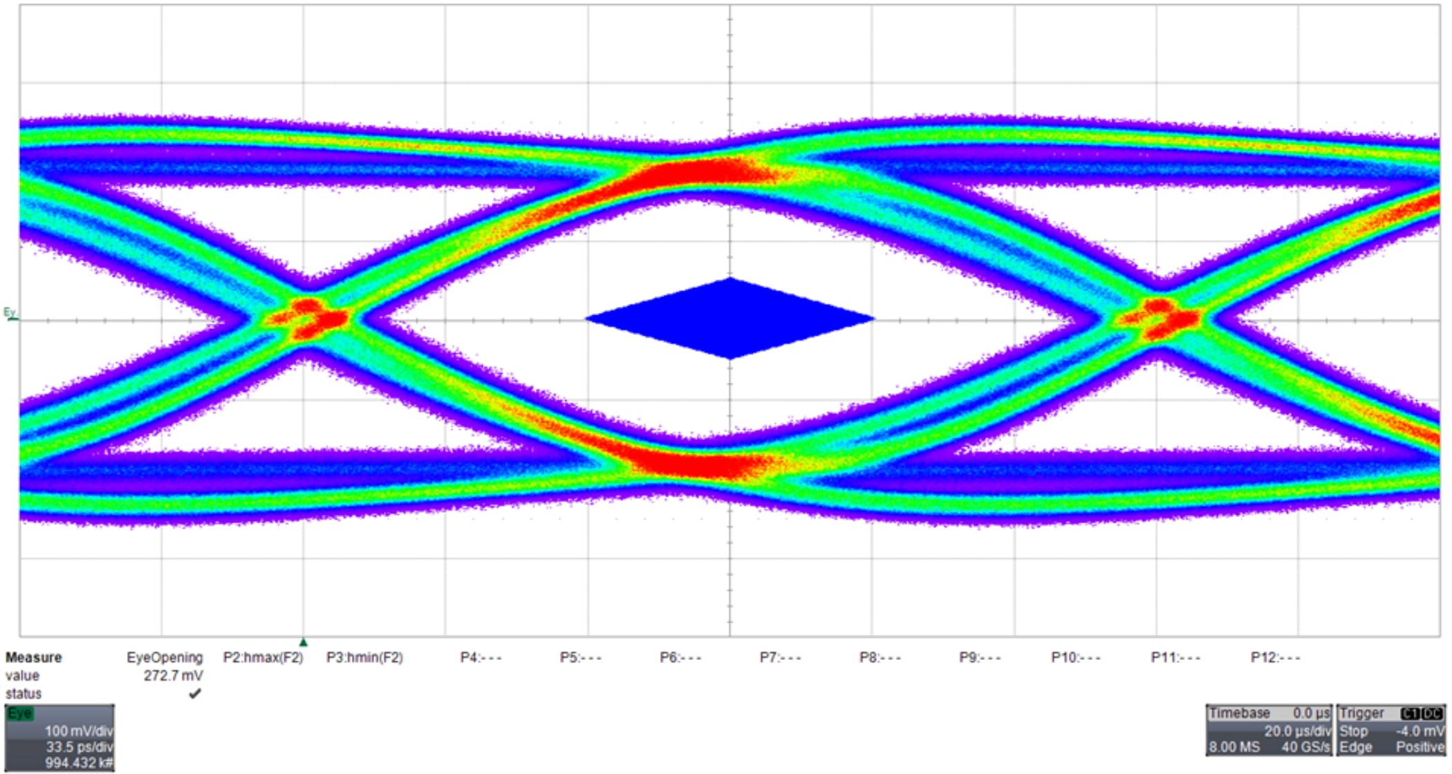 Figure 11. Eye Diagram for USB 3.0 Super-Speed Data Lines Using Single Layer Routing with Device Installed
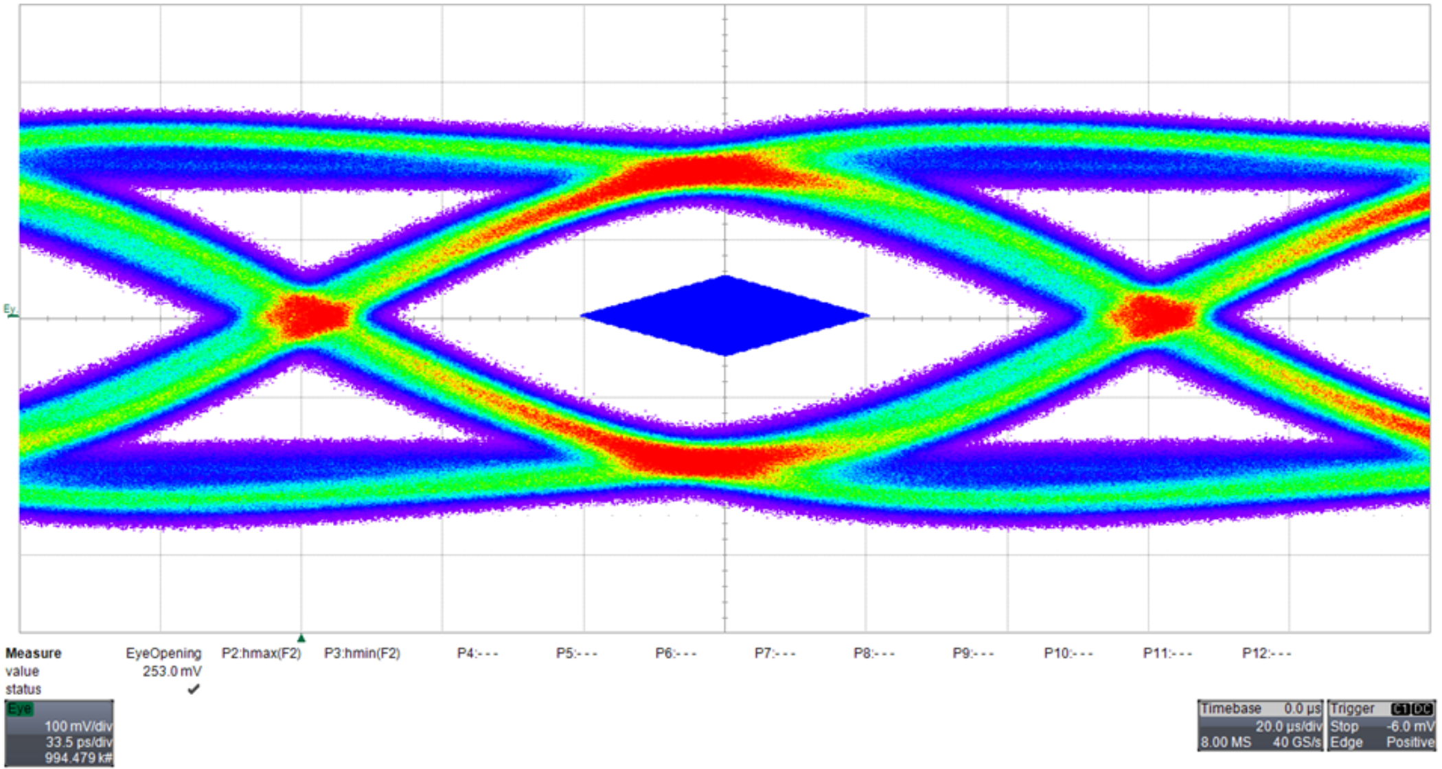 Figure 13. Eye Diagram for USB 3.0 Super-Speed Data Lines Using Double Layer Routing with Device Installed
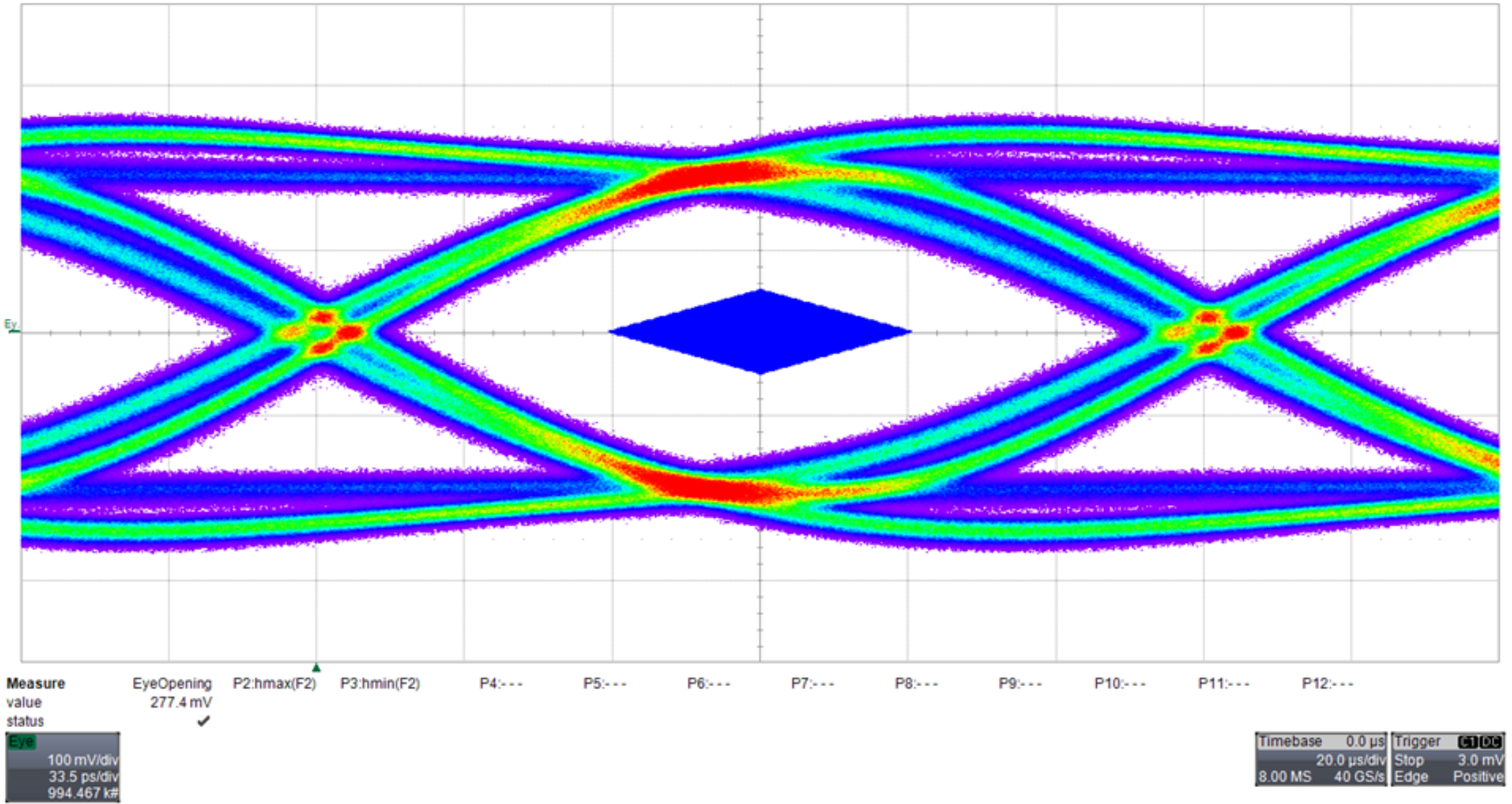 Figure 12. Eye Diagram for USB 3.0 Super-Speed Data Lines Using Single Layer Routing without Device Installed
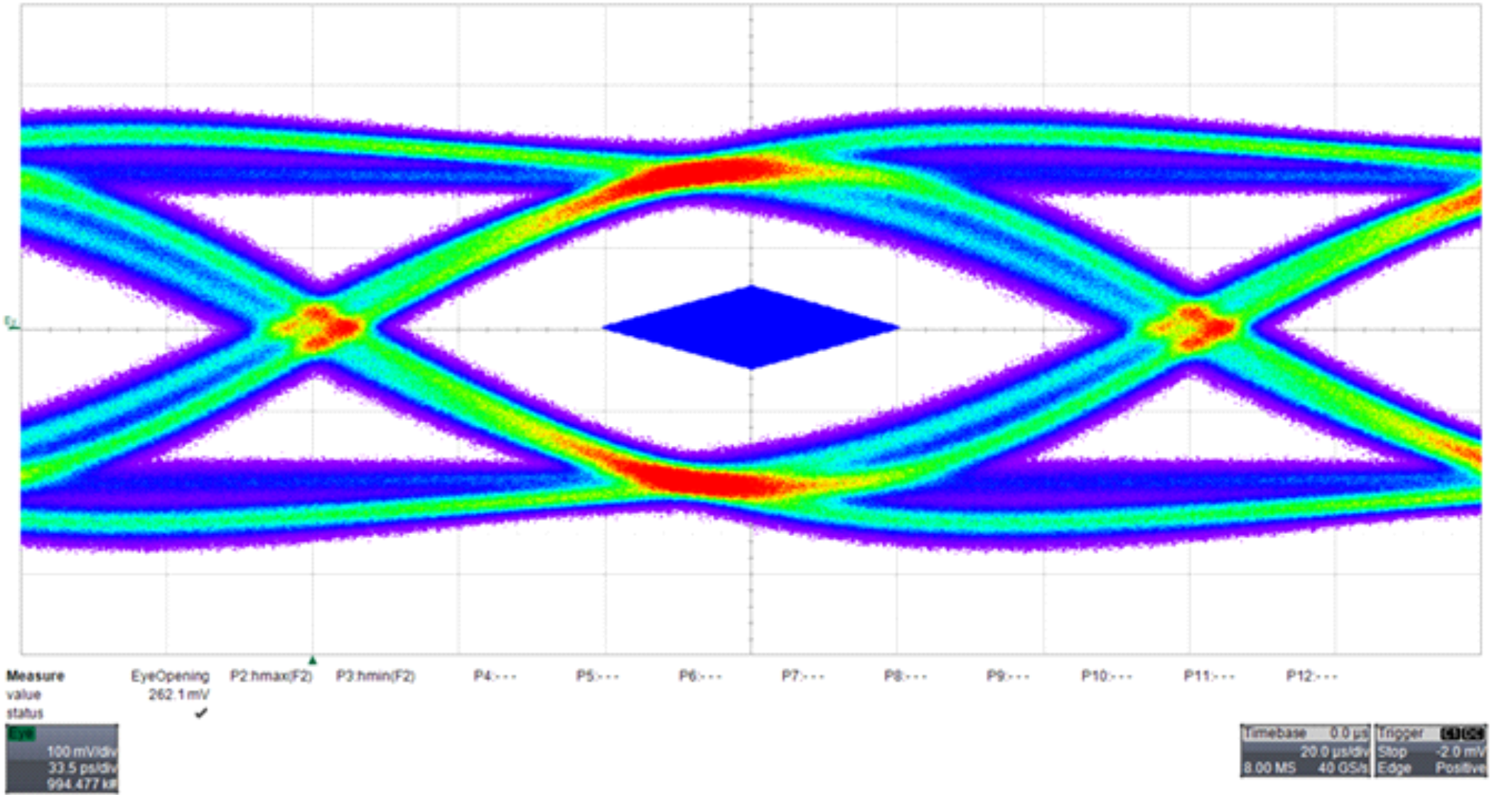 Figure 14. Eye Diagram for USB 3.0 Super-Speed Data Lines Using Double Layer Routing with Device Installed