SLVS788D February 2009 – November 2016 TPS22951
PRODUCTION DATA.
- 1 Features
- 2 Applications
- 3 Description
- 4 Revision History
- 5 Pin Configurations and Functions
- 6 Specifications
- 7 Parameter Measurement Information
- 8 Detailed Description
- 9 Application and Implementation
- 10Power Supply Recommendations
- 11Layout
- 12Device and Documentation Support
- 13Mechanical, Packaging, and Orderable Information
Package Options
Mechanical Data (Package|Pins)
- YFP|6
Thermal pad, mechanical data (Package|Pins)
Orderable Information
8 Detailed Description
8.1 Overview
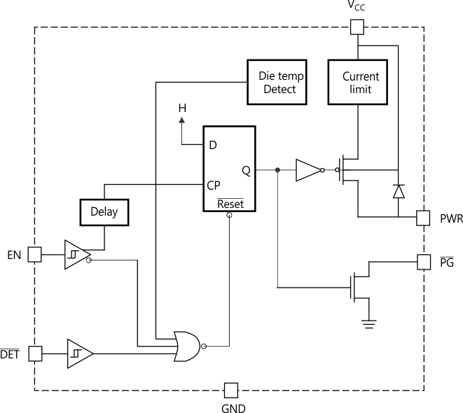
The TPS22951 smart-load switch is intended for applications where heavy capacitive loads and short circuits are likely to be encountered. This device incorporates a 1-Ω P-channel MOSFET power switch for power distribution. The switch is controlled by a logic enable (EN) input and an accessory detect (DET) pin. The switch is active when EN is high and DET is low. The switch is disabled if EN is low or DET is high. A low power state is achieved by driving EN low.
When the output load exceeds the current-limit threshold or a short is present, the device limits the output current to a safe level by increasing the on resistance of the power switch. When continuous heavy overloads and short circuits increase the power dissipation in the switch, causing the junction temperature to rise, a thermal-protection circuit shuts off the switch to prevent damage. The device recovers from a thermal shutdown once the device has cooled sufficiently, but the switch remains OFF until EN is toggled. This smart-load switch is designed to set current limit at 600 mA maximum.
8.2 Functional Block Diagram

8.3 Feature Description
8.3.1 Current Limit
The TPS22951 includes a current-limiting feature. The current limit can help protect the system from high currents in the case of large capacitive loads and short circuits. When the load current exceeds the current limit threshold, the device limits the output current by increasing the on-resistance of the switch.
8.3.2 Power Good Indication
The TPS22951 includes an open-drain Power Good indication. This signal can be used to provide an indication to another component in the system. The signal behaves according to Table 1.
To use the signal, the PG pin must be connected to a pullup resistor. The PG pin has an absolute maximum rating of 6 V and must not be pulled up to any voltage beyond 6 V. The pullp resistor must be in the range of 10 kΩ to limit the current flowing into the PG pin when the switch is on and the PG signal is low.
8.3.3 EN and DET inputs
The switch is controlled by the EN and DET pins. To enable the switch, the EN pin must be high and the DET pin must be low.
8.3.4 Thermal Shutdown
The TPS22951 includes a thermal shutdown circuit. If the device reaches the thermal shutdown threshold, the switch is automatically be disabled. The switch retrys after the device temperature has decreased and the EN pin is toggled from H to L to H.
8.4 Device Functional Modes
Table 1 lists the functional modes of the TPS22951.
Table 1. Function Table
| EN | DET | CURRENT LIMIT |
THERMAL LIMIT |
POWER SWITCH (VCC TO PWR) |
PG
(OPEN-DRAIN) |
|---|---|---|---|---|---|
| 0 | X | Not exceeded | Not exceeded | OFF | Z |
| X | 1 | Not exceeded | Not exceeded | OFF | Z |
| 1 | 0 | Not exceeded | Not exceeded | ON | L |
| 1 | 0 | Exceeded | Not exceeded | ON – current-limited | L |
| X | X | X | Exceeded (1) | OFF | Z |