SLVSBM6B December 2012 – November 2015 TPS22981
PRODUCTION DATA.
- 1 Features
- 2 Applications
- 3 Description
- 4 Revision History
- 5 Pin Configuration and Functions
- 6 Specifications
- 7 Detailed Description
- 8 Application and Implementation
- 9 Power Supply Recommendations
- 10Layout
- 11Device and Documentation Support
- 12Mechanical, Packaging, and Orderable Information
Package Options
Mechanical Data (Package|Pins)
- RGP|20
Thermal pad, mechanical data (Package|Pins)
- RGP|20
Orderable Information
8 Application and Implementation
NOTE
Information in the following applications sections is not part of the TI component specification, and TI does not warrant its accuracy or completeness. TI’s customers are responsible for determining suitability of components for their purposes. Customers should validate and test their design implementation to confirm system functionality.
8.1 Application Information
8.1.1 Input Inductive Bounce
When a significant inductance is seen at the VHV input, suddenly turning off large current through the device may produce a large enough inductive voltage bounce on the VHV pin to exceed the maximum safe operating condition and damage the TPS22981. To prevent this, reduce any inductance at the VHV input.
8.2 Typical Application
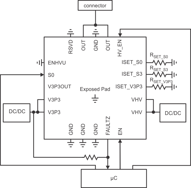
 Figure 9. Typical Application Schematic
8.2.1 Design Requirements
As the TPS22981 switches high-current levels, it is essential that all parallel output, power, and ground pins be connected. For example, ground connections must be provided on all ground pins including pins 1, 2, 3, 13, 15, and EP (the exposed package pad); both OUT pins (pins 12 and 14) must be connected; and so forth. RSET_S0, RSET_S3, and RSET_V3P3 must be determined using Equation 1. Unused inputs may not be left floating and should be connected to either ground or V3P3 depending on desired behavior.
8.2.2 Detailed Design Procedure
Design with TPS22981 is recommended as follows:
- Determine suitable current limits for the low-voltage and high-voltage output levels (output provided on the OUT pin). If S0 is being used, determine both high-voltage output levels and current-limiting values.
- Determine values for the resistors to be applied to pins ISET_V3P3, ISET_S3, and ISET_S0 using Equation 1 and the desired current limits determined above.
- If the FAULTZ output is being used, place a minimum 30-kΩ resistor (100-kΩ recommended) between FAULTZ and the V3P3.