SLVSBM6B December 2012 – November 2015 TPS22981
PRODUCTION DATA.
- 1 Features
- 2 Applications
- 3 Description
- 4 Revision History
- 5 Pin Configuration and Functions
- 6 Specifications
- 7 Detailed Description
- 8 Application and Implementation
- 9 Power Supply Recommendations
- 10Layout
- 11Device and Documentation Support
- 12Mechanical, Packaging, and Orderable Information
Package Options
Mechanical Data (Package|Pins)
- RGP|20
Thermal pad, mechanical data (Package|Pins)
- RGP|20
Orderable Information
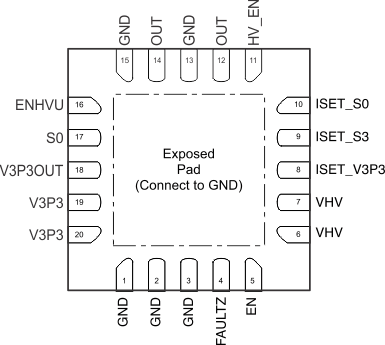
5 Pin Configuration and Functions
RGP Package
VQFN With Exposed Thermal Pad
Top View

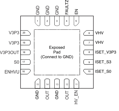
RGP Package
VQFN With Exposed Thermal Pad
Bottom View

Pin Functions
| PIN | TYPE | DESCRIPTION | |
|---|---|---|---|
| NAME | NO. | ||
| EN | 5 | I | Device active-high enable. |
| ENHVU | 16 | I | Enable VHV UVLO control of device enable. When asserted high, both V3P3 and VHV must be present for device enable. When low, only V3P3 must be present for device enable. |
| FAULTZ | 4 | O | Fault condition output. This pin is an open-drain pulldown indicating a fault condition. Place a pullup resistance (RFAULTZ) between this pin and V3P3. Float pin or tie pin to GND if unused. |
| GND | 1, 2, 3, 13, 15 | P | Device ground. All GND pins must be connected to board ground. |
| GND | EP | P | Exposed pad must be connected to device GND. |
| HV_EN | 11 | I | Active-high voltage output enable. |
| ISET_S0 | 10 | I | Sets the current limit for VHV in S0 mode. Place resistor between this pin and GND. See Equation 1 to calculate resistor value. |
| ISET_S3 | 9 | I | Sets the current limit for VHV in S3 mode. Place resistor between this pin and GND. See Equation 1 to calculate resistor value. |
| ISET_V3P3 | 8 | I | Sets the current limit for V3P3. Place resistor between this pin and GND. See Equation 1 to calculate resistor value. |
| OUT | 12, 14 | O | Power output. Place a minimum of 1-µF capacitor to GND as close to this pin as possible. |
| S0 | 17 | I | When this pin is asserted, the device is put in S0 mode. Otherwise the device operates in S3 mode. |
| V3P3 | 19, 20 | P | 3.3-V power supply input. Place a minimum of 0.1-µF capacitor to GND as close to this pin as possible. |
| V3P3OUT | 18 | O | 3.3-V bypass output. When ENHVU is low, this path is enabled by EN and the V3P3 UVLO. When ENHVU is high, this path is enabled by EN and both the V3P3 UVLO and the VHV UVLO. Place a minimum 0.1-uF capacitor to GND as close to this pin as possible. |
| VHV | 6, 7 | P | High voltage power supply input. See the Input Inductive Bounce section for more information. |