SLVSEG3E September 2019 – March 2022 TPS25840-Q1 , TPS25842-Q1
PRODUCTION DATA
- 1 Features
- 2 Applications
- 3 Description
- 4 Revision History
- 5 Description (Continued)
- 6 Device Comparison Table
- 7 Pin Configuration and Functions
- 8 Specifications
- 9 Parameter Measurement Information
-
10Detailed Description
- 10.1 Overview
- 10.2 Functional Block Diagram
- 10.3
Feature Description
- 10.3.1 Buck Regulator
- 10.3.2 Enable/UVLO
- 10.3.3 Switching Frequency and Synchronization (RT/SYNC)
- 10.3.4 Spread-Spectrum Operation
- 10.3.5 VCC, VCC_UVLO
- 10.3.6 Minimum ON-time, Minimum OFF-time
- 10.3.7 Internal Compensation
- 10.3.8 Bootstrap Voltage (BOOT)
- 10.3.9 RSNS, RSET, RILIMIT and RIMON
- 10.3.10 Overcurrent and Short Circuit Protection
- 10.3.11 Overvoltage, IEC and Short-to-Battery Protection
- 10.3.12 Cable Compensation
- 10.3.13 USB Port Control
- 10.3.14 FAULT Response
- 10.3.15 USB Specification Overview
- 10.3.16 Device Power Pins (IN, CSN/OUT, and PGND)
- 10.3.17 Thermal Shutdown
- 10.4 Device Functional Modes
-
11Application and Implementation
- 11.1 Application Information
- 11.2
Typical Application
- 11.2.1 Design Requirements
- 11.2.2
Detailed Design Procedure
- 11.2.2.1 Output Voltage
- 11.2.2.2 Switching Frequency
- 11.2.2.3 Inductor Selection
- 11.2.2.4 Output Capacitor Selection
- 11.2.2.5 Input Capacitor Selection
- 11.2.2.6 Bootstrap Capacitor Selection
- 11.2.2.7 VCC Capacitor Selection
- 11.2.2.8 Enable and Under Voltage Lockout Set-Point
- 11.2.2.9 Current Limit Set-Point
- 11.2.2.10 Cable Compensation Set-Point
- 11.2.2.11 FAULT Resistor Selection
- 11.2.3 Application Curves
- 12Power Supply Recommendations
- 13Layout
- 14Device and Documentation Support
- 15Mechanical, Packaging, and Orderable Information
Package Options
Mechanical Data (Package|Pins)
- RHB|32
Thermal pad, mechanical data (Package|Pins)
- RHB|32
Orderable Information
10.3.10.1 Current Limit Setting using RILIMIT
Refer to Figure 10-14. The TPS2584x-Q1 can establish current limit by two methods.
- Using external a single or back-to-back N-Channel MOFETs between CSN/OUT and BUS: a voltage of 0.49 V on the ILIMIT pin initiates current limiting using the external MOSFET by decreasing the LS_GD voltage causing the FET to operate in the saturation region. To protect the MOSFETs from damage a hiccup timer limits the duty cycle to prevent thermal runaway. Refer to the Specifications for MOSFET hiccup timing.
- Buck average current limit: no MOSFET, CSN/OUT connected to BUS. The LS_GD must be pulled up through a 2.2-kΩ resistor. In this configuration, a voltage of 1 V across RILIMIT on the ILIMIT pin initiates average current limiting of the buck regulator.
The 2-level current limit is described below:
- With external MOSFET Figure 10-15:
-
Isolating a fault on the USB port from other loads connected to the CSP output of the TPS2584x-Q1. In some applications, it can be useful to power additional circuitry (for example: USB HUB) from the output of the TPS2584x-Q1 and maintain operation of these circuits in the event of a short circuit downstream of the BUS pin. To prevent triggering the MOSFET current limit below the programmed ILIMIT threshold, external circuits must be supplied after the inductor and before the current sense resistor, RSNS.
-
After RSNS and RSET are determined and the full load ISET current is known, the resistor value, RILIMIT, can be determined by:
Equation 6.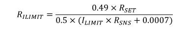
-
In most cases, the recommended voltage across RSNS under current limit must be approximately 50 mV as a compromise between accuracy and power dissipation. While in some application, RILIMIT is the only resistor that can be changed to achieve different current limit. Typical RILIMIT resistors value are listed in Table 10-2 given the condition RSNS = 15 mΩ and RSET = 300 Ω
Table 10-2 Setting the Current Limit with RILIMITCurrent-Limit Threshold (mA) RILIMIT (kΩ) With External MOSFET Without External MOSFET 700 26.1 53.6 1500 12.7 26.1 1700 11.3 22.6 2700 7.15 14.7 3000 6.49 13 3400 5.62 11.5 3800 5.11 10.5
-
- Buck Average Current Limit Figure 10-16:
-
CSN/OUT connected directly to BUS, LS_GD must be pulled up through 2.2-kΩ resistor. The TPS2584x-Q1 can operate as a stand-alone USB charging port. In this configuration, the internal buck regulator operates with average current limiting as programmed by the ILIMIT pin, potentially producing less heat compared to N-channel MOSFET current limiting
-
After RSNS and RSET are determined and the full load ISET current is known, the resistor value RILIMIT can be determined by:
Equation 7.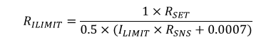
-
Table 10-2 lists Typical RILIMIT resistors values given the condition RSNS = 15 mΩ and RSET = 300 Ω.
-
 Figure 10-15 Current Limit With External MOSFET
 Figure 10-16 Buck Average Current Limit