SLUS710E May   2006  – January 2024 TPS28225

PRODUCTION DATA  

  1.   1
  2. Features
  3. Applications
  4. Description
  5. Pin Configuration and Functions
  6. Specifications
    1. 5.1 Absolute Maximum Ratings
    2. 5.2 ESD Ratings
    3. 5.3 Recommended Operating Conditions
    4. 5.4 Thermal Information
    5. 5.5 Electrical Characteristics
    6. 5.6 Switching Characteristics
    7. 5.7 Typical Characteristics
  7. Detailed Description
    1. 6.1 Overview
    2. 6.2 Functional Block Diagram
    3. 6.3 Feature Description
      1. 6.3.1 Undervoltage Lockout (UVLO)
      2. 6.3.2 Output Active Low
      3. 6.3.3 Enable/Power Good
      4. 6.3.4 3-State Input
        1. 6.3.4.1 TPS28225 3-State Exit Mode
        2. 6.3.4.2 External Resistor Interference
      5. 6.3.5 Bootstrap Diode
      6. 6.3.6 Upper and Lower Gate Drivers
      7. 6.3.7 Dead-Time Control
      8. 6.3.8 Thermal Shutdown
    4. 6.4 Device Functional Modes
  8. Application and Implementation
    1. 7.1 Application Information
    2. 7.2 Typical Application
      1. 7.2.1 Design Requirements
      2. 7.2.2 Detailed Design Procedure
        1. 7.2.2.1 Four Phases Driven by TPS28225 Driver
        2. 7.2.2.2 Switching The MOSFETs
        3. 7.2.2.3 List of Materials
      3. 7.2.3 Application Curves
    3. 7.3 System Examples
  9. Power Supply Recommendations
  10. Layout
    1. 9.1 Layout Guidelines
    2. 9.2 Layout Example
  11. 10Device and Documentation Support
    1. 10.1 Device Support
      1. 10.1.1 Third-Party Products Disclaimer
    2. 10.2 Documentation Support
      1. 10.2.1 Related Documentation
    3. 10.3 Receiving Notification of Documentation Updates
    4. 10.4 Support Resources
    5. 10.5 Trademarks
    6. 10.6 Electrostatic Discharge Caution
    7. 10.7 Glossary
  12. 11Revision History
  13. 12Mechanical, Packaging, and Orderable Information

Package Options

Mechanical Data (Package|Pins)
Thermal pad, mechanical data (Package|Pins)
Orderable Information

Typical Characteristics

GUID-2D61B4F2-E6F1-4271-86F9-56E062661CF7-low.gif
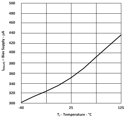
VEN/PG = LowPWM Input FloatingVDD = 7.2 V
Figure 5-2 Bias Supply Current vs Temperature
GUID-ED7971F5-1BF5-4E1C-AAE9-C57862021F17-low.gif
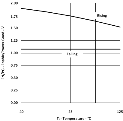
VDD = 7.2 V
Figure 5-4 Enable/Power Good Threshold vs Temperature
GUID-37B2232C-18DB-46DC-AF6A-54B860C51F19-low.gif
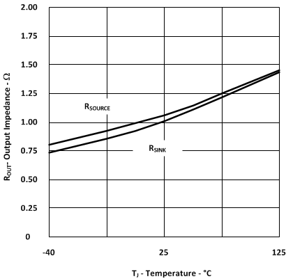
VDD = 7.2 V
Figure 5-6 UGATE DC Output Impedance vs Temperature
GUID-5F232D6D-0170-4C5B-963F-ACE3E7D87A81-low.gif
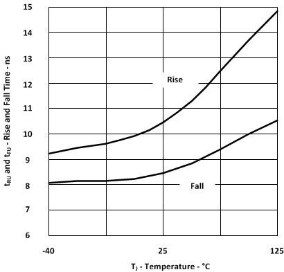
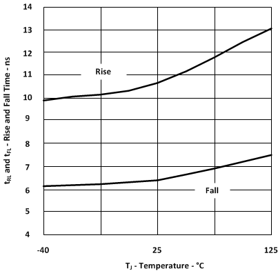
VDD = 7.2 VCLOAD = 3 nF
Figure 5-8 UGATE Rise and Fall Time vs Temperature
GUID-F3CBC794-A8E7-4D5A-8C65-FF89F128A588-low.gif
VDD = 7.2 VCLOAD = 3 nF
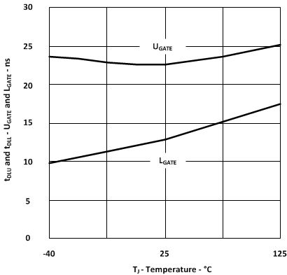
Figure 5-10 UGATE and LGATE (Turning OFF Propagation Delays) vs Temperture
GUID-8977EACF-DD3A-42D9-A062-A6AF52BCDD2C-low.gif
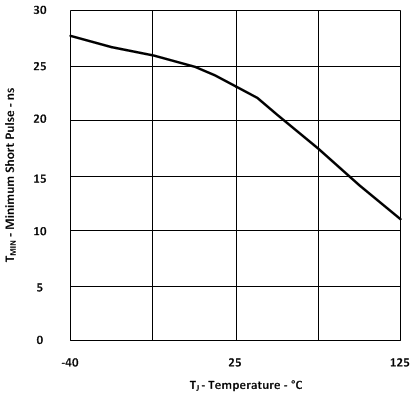
VDD = 7.2 VCLOAD = 3 nF
Figure 5-12 UGATE Minimum Short Pulse vs Temperature
GUID-212271ED-0880-4CF3-8429-5F8A12233E31-low.gif
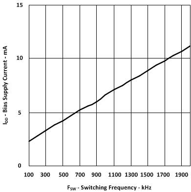
No LoadVDD = 7.2 VTJ = 25°C
Figure 5-14 Bias Supply Current vs Switching Frequency
GUID-ADDF5D76-9083-48E3-984E-E97088DF32D5-low.gif
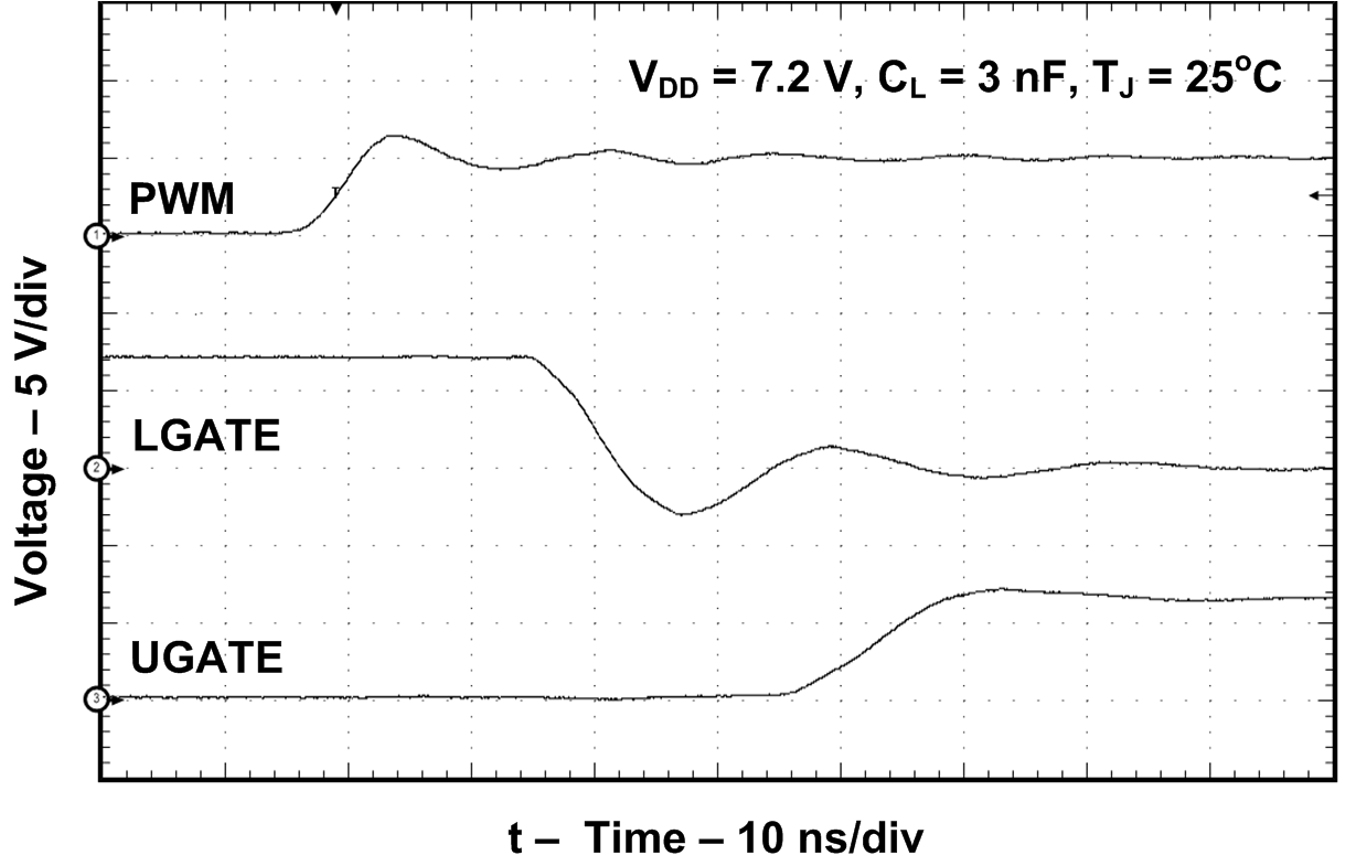
Figure 5-16 PWM Input Rising Switching Waveforms
GUID-227748C1-71EE-47DC-898D-BD7CA0224280-low.gif
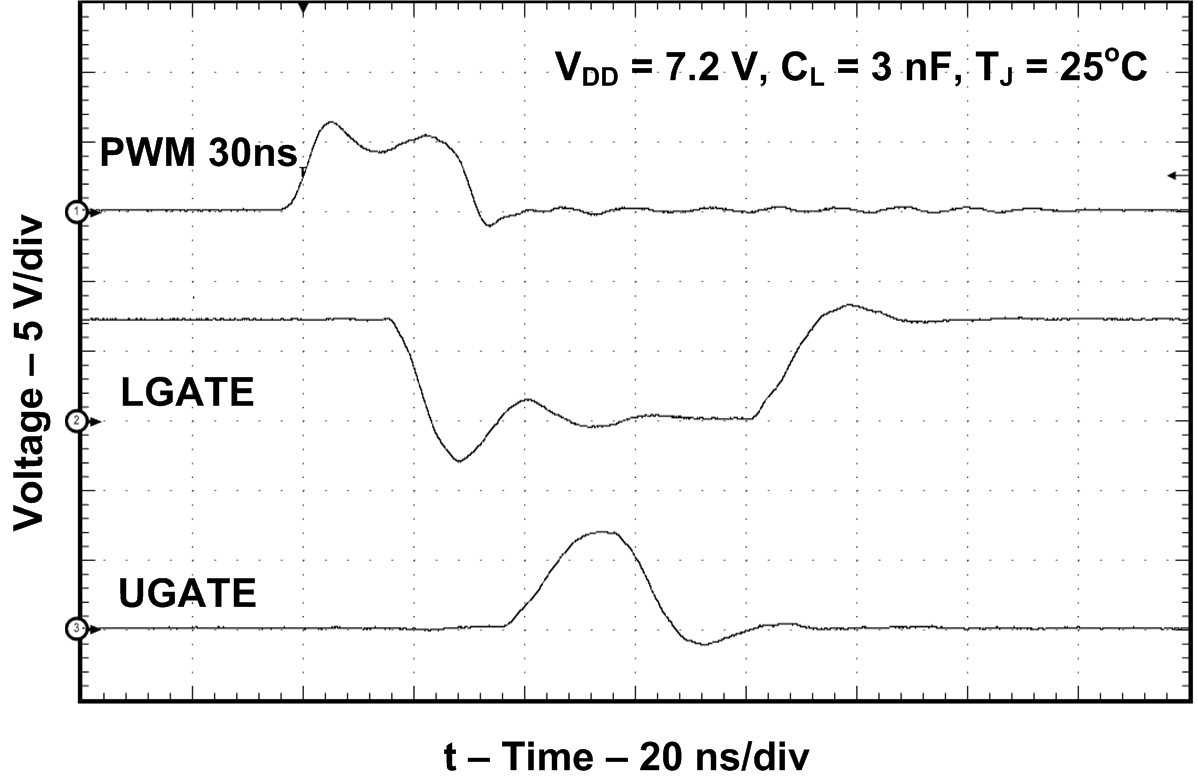
Figure 5-18 Minimum UGATE Pulse Switching Waveforms
GUID-E5194222-7C3F-40C4-A407-5360EC93BF7E-low.gif
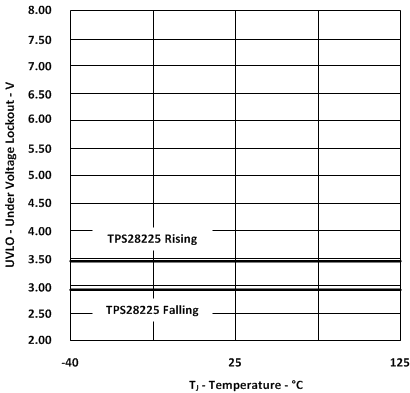
Figure 5-3 Undervoltage Lockout Threshold vs Temperature
GUID-86447147-74C8-481E-A274-512104396A81-low.gif
VDD = 7.2 V
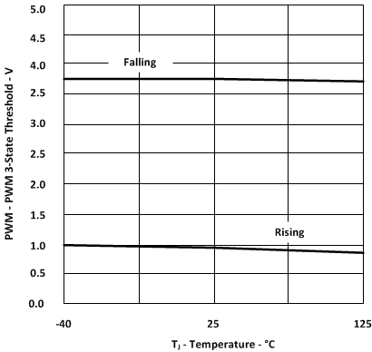
Figure 5-5 PWM 3-State Thresholds, (5-V Input Pulses) vs Temperature
GUID-4C1A63E5-12C5-4E15-8B9A-901944972038-low.gif
VDD = 7.2 V
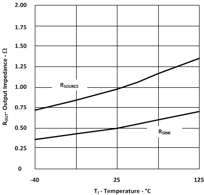
Figure 5-7 LGATE DC Output Impedance vs Temperature
GUID-73A24D3B-E481-4836-A0A7-BAC5886A86B2-low.gif
VDD = 7.2 VCLOAD = 3 nF
Figure 5-9 LGATE Rise and Fall Time vs Temperature
GUID-FE9C5D34-36CC-491F-BB15-C85BB9077DA4-low.gif
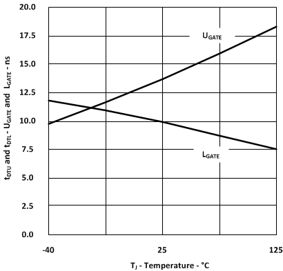
VDD = 7.2 VCLOAD = 3 nF
Figure 5-11 UGATE and LGATE (Dead Time) vs Temperture
GUID-2FECB67F-D81F-4DE1-9926-E5BFC3930242-low.gif
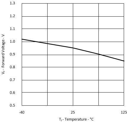
VDD = 7.2 VIF = 100 mA
Figure 5-13 Bootstrap Diode Forward Voltage vs Temperature
GUID-0DB906C9-09C3-42A0-988B-4DCD39A543F0-low.gif
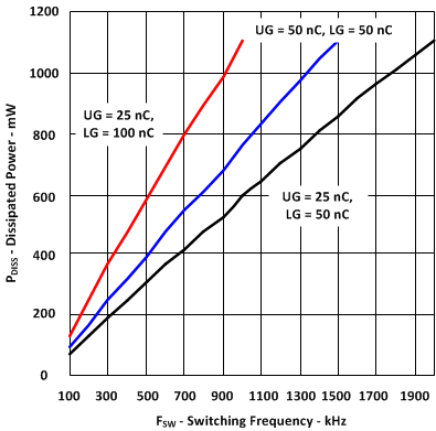
Different Load ChargeVDD = 7.2 VTJ = 25°C
Figure 5-15 Driver Dissipated Power vs Switching Frequency
GUID-A2CDD27F-9DD2-4D23-844F-76457A2013BA-low.gif
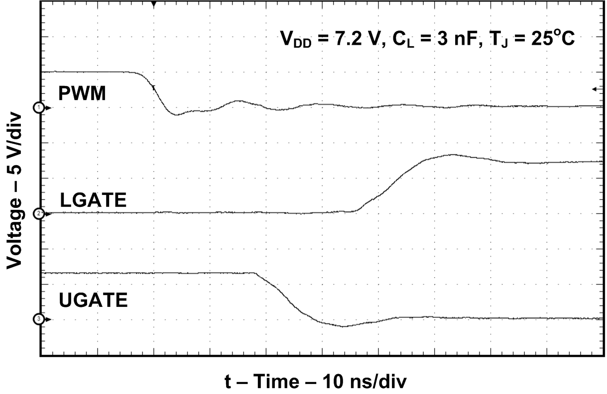
Figure 5-17 PWM Input Falling Switching Waveforms
GUID-00E7E52E-F821-4723-BC99-AFE42EE73F9C-low.gif
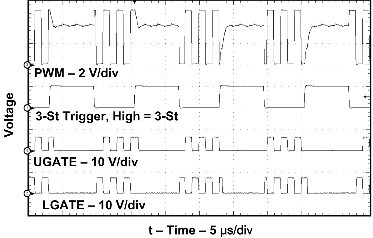
Figure 5-19 Normal and 3-State Operation Enter/Exit Conditions