SBVS103D April 2008 – December 2014 TPS3808-EP
PRODUCTION DATA.
- 1 Features
- 2 Applications
- 3 Description
- 4 Revision History
- 5 Pin Configuration and Functions
- 6 Specifications
- 7 Detailed Description
- 8 Application and Implementation
- 9 Power Supply Recommendations
- 10Layout
- 11Device and Documentation Support
- 12Mechanical, Packaging, and Orderable Information
Package Options
Mechanical Data (Package|Pins)
- DBV|6
Thermal pad, mechanical data (Package|Pins)
Orderable Information
8 Application and Implementation
NOTE
Information in the following applications sections is not part of the TI component specification, and TI does not warrant its accuracy or completeness. TI’s customers are responsible for determining suitability of components for their purposes. Customers should validate and test their design implementation to confirm system functionality.
8.1 Application Information
The following sections describe in detail how to properly use this device depending on the requirements of the final application.
8.1.1 SENSE Input
The SENSE input provides a terminal at which any system voltage can be monitored. If the voltage on this pin drops below VIT, then RESET is asserted. The comparator has a built-in hysteresis to ensure smooth RESET assertions and de-assertions. It is good analog design practice to put a 1-nF to 10-nF bypass capacitor on the SENSE input to reduce sensitivity to transients and layout parasitics.
The TPS3808 device is relatively immune to short negative transients on the SENSE pin. Sensitivity to transients is dependent on threshold overdrive, as shown in the Maximum Transient Duration at Sense vs Sense Threshold Overdrive Voltage graph (Figure 5) in Typical Characteristics.
The TPS3808G01 can be used to monitor any voltage rail down to 0.405 V using the circuit shown in Figure 9.
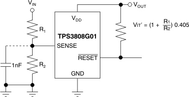 Figure 9. Using the TPS3808G01 to Monitor a User-Defined Threshold Voltage
8.1.2 Selecting the RESET Delay Time
The TPS3808 has three options for setting the RESET delay time as shown in Figure 10. Figure 10a shows the configuration for a fixed 300-ms typical delay time by tying CT to VDD; a resistor from 40 kΩ to 200 kΩ must be used. Supply current is not affected by the choice of resistor. Figure 10b shows a fixed 20-ms delay time by leaving the CT pin open. Figure 10c shows a ground referenced capacitor connected to CT for a user-defined program time between 1.25 ms and 10 s.
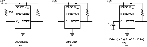 Figure 10. Configuration Used to Set the RESET Delay Time
The capacitor CT should be ≥ 100 pF nominal value in order for the TPS3808xxx to recognize that the capacitor is present. The capacitor value for a given delay time can be calculated using Equation 1.

The reset delay time is determined by the time it takes an on-chip precision 220-nA current source to charge the external capacitor to 1.23 V. When a RESET is asserted the capacitor is discharged. When the RESET conditions are cleared, the internal current source is enabled and begins to charge the external capacitor. When the voltage on this capacitor reaches 1.23 V, RESET is deasserted. Note that a low-leakage type capacitor such as a ceramic should be used, and that stray capacitance around this pin may cause errors in the reset delay time.
8.1.3 Manual RESET(MR) Input
The manual reset (MR) input allows a processor or other logic circuits to initiate a reset. A logic low (0.3 VDD) on MR causes RESET to assert. After MR returns to a logic high and SENSE is above its reset threshold, RESET is de-asserted after the user defined reset delay expires. Note that MR is internally tied to VDD using a 90-kΩ resistor so this pin can be left unconnected if MR will not be used.
See Figure 11 for how MR can be used to monitor multiple system voltages. Note that if the logic signal driving MR does not go fully to VDD, there will be some additional current draw into VDD as a result of the internal pullup resistor on MR. To minimize current draw, a logic-level FET can be used as illustrated in Figure 12.
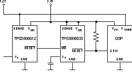 Figure 11. Using MR to Monitor Multiple System Voltages
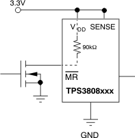 Figure 12. Using an External MOSFET to Minimize IDD When MR Signal Does Not Go to VDD
8.1.4 RESET Output
RESET remains high (unasserted) as long as SENSE is above its threshold (VIT) and the manual reset (MR) is logic high. If either SENSE falls below VIT or MR is driven low, RESET is asserted, driving the RESET pin to a low impedance.
Once MR is again logic high and SENSE is above VIT + VHYS (the threshold hysteresis), a delay circuit is enabled which holds RESET low for a specified reset delay period. Once the reset delay has expired, the RESET pin goes to a high impedance state. The pullup resistor from the open-drain RESET to the supply line can be used to allow the reset signal for the microprocessor to have a voltage higher than VDD (up to 6.5 V). The pullup resistor should be no smaller than 10 kΩ as a result of the finite impedance of the RESET line.
8.2 Typical Application
A typical application of the TPS3808G33 used with a 3.3 V processor is shown in Figure 13. The open-drain RESET output is typically connected to the RESET input of a microprocessor. A pullup resistor must be used to hold this line high when RESET is not asserted. The RESET output is undefined for voltage below 0.8 V, but this is normally not a problem since most microprocessors do not function below this voltage.
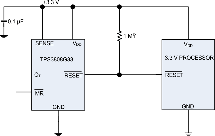 Figure 13. Typical Application of the TPS3808 with a 3.3 V Processor
8.2.1 Design Requirements
The TPS3808 is intended to drive the RESET input of a microprocessor. The RESET pin is pulled high with a 1 MΩ resistor and the reset delay time is controlled by CT depending on the reset requirement times of the microprocessor. In this case, CT is left open for a typical reset delay time of 20 ms.
8.2.2 Detailed Design Procedure
The main constraint for this application is the reset delay time. In this case, since CT is open, it is set to 20 ms. A 0.1 µF decoupling capacitor is connected to the VDDpin and a 1 MΩ resistor is used to pull-up the RESET pin high. The MR pin can be connected to an external signal if desired.
8.2.3 Application Curve
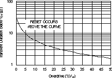 Figure 14. Maximum Transient Duration at Sense vs Sense Threshold Overdrive Voltage