SBVS103D April 2008 – December 2014 TPS3808-EP
PRODUCTION DATA.
- 1 Features
- 2 Applications
- 3 Description
- 4 Revision History
- 5 Pin Configuration and Functions
- 6 Specifications
- 7 Detailed Description
- 8 Application and Implementation
- 9 Power Supply Recommendations
- 10Layout
- 11Device and Documentation Support
- 12Mechanical, Packaging, and Orderable Information
Package Options
Mechanical Data (Package|Pins)
- DBV|6
Thermal pad, mechanical data (Package|Pins)
Orderable Information
10 Layout
10.1 Layout Guidelines
Make sure the connection to the VDD pin is low impedance. Place a 0.1-µF ceramic capacitor near the VDD pin.
10.2 Layout Example
The layout example in Figure 15 shows how the TPS3808 is laid out on a PCB for a 20 ms delay.
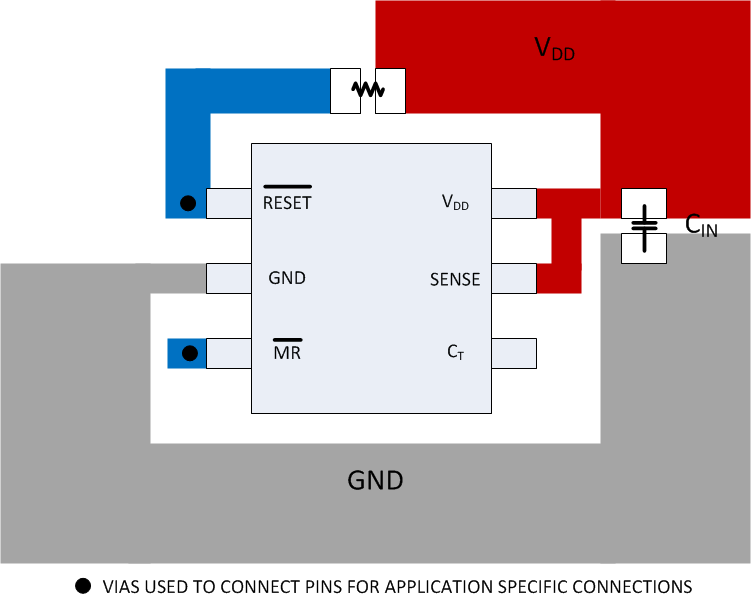 Figure 15. Layout Example for a 20 ms Delay