SBVS050M May 2004 – March 2023 TPS3808
PRODUCTION DATA
- 1 Features
- 2 Applications
- 3 Description
- 4 Revision History
- 5 Device Voltage Thresholds
- 6 Pin Configuration and Functions
- 7 Specifications
- 8 Detailed Description
- 9 Application and Implementation
- 10Power Supply Recommendations
- 11Layout
- 12Device and Documentation Support
- 13Mechanical, Packaging, and Orderable Information
Package Options
Mechanical Data (Package|Pins)
Thermal pad, mechanical data (Package|Pins)
- DRV|6
Orderable Information
8.3.1 SENSE Input
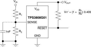
The SENSE input provides a pin at which any system voltage can be monitored. If the voltage on this pin drops below VIT, then RESET is asserted. The comparator has a built-in hysteresis to ensure smooth RESET assertions and de-assertions. It is good analog design practice to put a 1-nF to 10-nF bypass capacitor on the SENSE input to reduce sensitivity to transients and layout parasitics.
The TPS3808 device is relatively immune to short negative transients on the SENSE pin. Sensitivity to transients is dependent on threshold overdrive, as shown in (GUID-2C45C6A6-DA12-46ED-9D40-BB37409EA452.html#SBVS037FIG3016).
The TPS3808G01 can be used to monitor any voltage rail down to 0.405 V using the circuit shown in #SBVS050IMG9889.
 Figure 8-1 Using the TPS3808G01 to Monitor a User-Defined Threshold Voltage