SLVSB90C January 2012 – November 2023 TPS40170-Q1
PRODUCTION DATA
- 1
- 1 Features
- 2 Applications
- 3 Description
- 4 Pin Configuration and Functions
- 5 Specifications
-
6 Detailed Description
- 6.1 Overview
- 6.2 Functional Block Diagram
- 6.3
Feature Description
- 6.3.1 LDO Linear Regulators and Enable
- 6.3.2 Input Undervoltage Lockout (UVLO)
- 6.3.3 Equations for Programming the Input UVLO
- 6.3.4 Overcurrent Protection and Short-Circuit Protection (OCP and SCP)
- 6.3.5 Oscillator and Voltage Feed-Forward
- 6.3.6 Feed-Forward Oscillator Timing Diagram
- 6.3.7 Soft-Start and Fault-Logic
- 6.3.8 Overtemperature Fault
- 6.3.9 Tracking
- 6.3.10 Adaptive Drivers
- 6.3.11 Start-Up Into Pre-Biased Output
- 6.3.12 31
- 6.3.13 Power Good (PGOOD)
- 6.3.14 PGND and AGND
- 6.3.15 Bootstrap Capacitor
- 6.3.16 Bypass and Filtering
- 6.4 Device Functional Modes
-
7 Application and Implementation
- 7.1 Application Information
- 7.2
Typical Application
- 7.2.1 Design Requirements
- 7.2.2
Detailed Design Procedure
- 7.2.2.1 Select A Switching Frequency
- 7.2.2.2 Inductor Selection (L1)
- 7.2.2.3 Output Capacitor Selection (C9)
- 7.2.2.4 Peak Current Rating of Inductor
- 7.2.2.5 Input Capacitor Selection (C1, C6)
- 7.2.2.6 MOSFET Switch Selection (Q1, Q2)
- 7.2.2.7 Timing Resistor (R7)
- 7.2.2.8 UVLO Programming Resistors (R2, R6)
- 7.2.2.9 Bootstrap Capacitor (C7)
- 7.2.2.10 VIN Bypass Capacitor (C18)
- 7.2.2.11 VBP Bypass Capacitor (C19)
- 7.2.2.12 SS Timing Capacitor (C15)
- 7.2.2.13 ILIM Resistor (R19, C17)
- 7.2.2.14 SCP Multiplier Selection (R5)
- 7.2.2.15 Feedback Divider (R10, R11)
- 7.2.2.16 Compensation: (R4, R13, C13, C14, C21)
- 7.2.3 Application Curves
- 7.3 Power Supply Recommendations
- 7.4 Layout
- 8 Device and Documentation Support
- 9 Revision History
- 10Mechanical, Packaging, and Orderable Information
Package Options
Mechanical Data (Package|Pins)
- RGY|20
Thermal pad, mechanical data (Package|Pins)
- RGY|20
Orderable Information
6.3.5 Oscillator and Voltage Feed-Forward
TPS40170-Q1 device implements an oscillator with input-voltage feed-forward compensation that enables instant response to input voltage changes. Figure 6-4 shows the oscillator timing diagram for the TPS40170-Q1 device. The resistor from the RT pin to GND sets the free-running oscillator frequency. Voltage VRT on the RT pin is made proportional to the input voltage (see Equation 5).
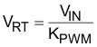
where
- K = 15
The resistor at the RT pin sets the current in the RT pin. The proportional current charges an internal 100-pF oscillator capacitor. The ramp voltage on this capacitor is compared with the RT pin voltage, VRT. Once the ramp voltage reaches VRT, the oscillator capacitor is discharged. The ramp that is generated by the oscillator (which is proportional to the input voltage) acts as voltage feed-forward ramp to be used in the PWM comparator.
The time between the start of the discharging oscillator capacitor and the start of the next charging cycle is fixed at 170 ns (typical). During the fixed discharge time, the PWM output is maintained as OFF. This is the minimum OFF-time of the PWM output.
 Figure 6-4 Feed-Forward Oscillator Timing Diagram