SLVSB90C January 2012 – November 2023 TPS40170-Q1
PRODUCTION DATA
- 1
- 1 Features
- 2 Applications
- 3 Description
- 4 Pin Configuration and Functions
- 5 Specifications
-
6 Detailed Description
- 6.1 Overview
- 6.2 Functional Block Diagram
- 6.3
Feature Description
- 6.3.1 LDO Linear Regulators and Enable
- 6.3.2 Input Undervoltage Lockout (UVLO)
- 6.3.3 Equations for Programming the Input UVLO
- 6.3.4 Overcurrent Protection and Short-Circuit Protection (OCP and SCP)
- 6.3.5 Oscillator and Voltage Feed-Forward
- 6.3.6 Feed-Forward Oscillator Timing Diagram
- 6.3.7 Soft-Start and Fault-Logic
- 6.3.8 Overtemperature Fault
- 6.3.9 Tracking
- 6.3.10 Adaptive Drivers
- 6.3.11 Start-Up Into Pre-Biased Output
- 6.3.12 31
- 6.3.13 Power Good (PGOOD)
- 6.3.14 PGND and AGND
- 6.3.15 Bootstrap Capacitor
- 6.3.16 Bypass and Filtering
- 6.4 Device Functional Modes
-
7 Application and Implementation
- 7.1 Application Information
- 7.2
Typical Application
- 7.2.1 Design Requirements
- 7.2.2
Detailed Design Procedure
- 7.2.2.1 Select A Switching Frequency
- 7.2.2.2 Inductor Selection (L1)
- 7.2.2.3 Output Capacitor Selection (C9)
- 7.2.2.4 Peak Current Rating of Inductor
- 7.2.2.5 Input Capacitor Selection (C1, C6)
- 7.2.2.6 MOSFET Switch Selection (Q1, Q2)
- 7.2.2.7 Timing Resistor (R7)
- 7.2.2.8 UVLO Programming Resistors (R2, R6)
- 7.2.2.9 Bootstrap Capacitor (C7)
- 7.2.2.10 VIN Bypass Capacitor (C18)
- 7.2.2.11 VBP Bypass Capacitor (C19)
- 7.2.2.12 SS Timing Capacitor (C15)
- 7.2.2.13 ILIM Resistor (R19, C17)
- 7.2.2.14 SCP Multiplier Selection (R5)
- 7.2.2.15 Feedback Divider (R10, R11)
- 7.2.2.16 Compensation: (R4, R13, C13, C14, C21)
- 7.2.3 Application Curves
- 7.3 Power Supply Recommendations
- 7.4 Layout
- 8 Device and Documentation Support
- 9 Revision History
- 10Mechanical, Packaging, and Orderable Information
Package Options
Mechanical Data (Package|Pins)
- RGY|20
Thermal pad, mechanical data (Package|Pins)
- RGY|20
Orderable Information
6.3.9 Tracking
The TRK pin is used for output voltage tracking. The output voltage is regulated so that the FB pin equals the lowest of the internal reference voltage (VREF) or the level-shifted SS pin voltage (SSEAMP) or the TRK pin voltage. Once the TRK pin goes above the reference voltage, then the output voltage is no longer governed by the TRK pin, but it is governed by the reference voltage.
If the voltage tracking function is used, then it must be noted that the SS pin capacitor must remain connected to SS pin and is also used for FAULT timing. For proper tracking using the TRK pin, the tracking voltage must be allowed to rise only after SSEAMP has exceeded VREF, so that there is no possibility of the TRK pin voltage being higher than the SSEAMP voltage. From Figure 6-6, for SSEAMP = 0.6 V, the SS pin voltage is typically 1.7 V.
The maximum slew rate on the TRK pin must be determined by the output capacitance and feedback loop bandwidth. A higher slew rate can possibly trip overcurrent protection.
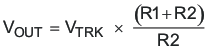
Figure 6-9 shows the tracking functional block. For SSEAMP voltages greater than TRK pin voltage, the VOUT is given by Equation 12 and Equation 13.
For 0 V < VTRK < VREF
For VTRK > VREF
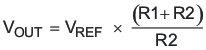
 Figure 6-9 Tracking Functional Block
There are three potential applications for the tracking function.
- Simultaneous voltage tracking
- Ratiometric voltage tracking
- Sequential start-up mode
The tracking function configurations and waveforms are shown in Figure 6-10, Figure 6-11, Figure 6-12, Figure 6-13, Figure 6-14, and Figure 6-15 respectively.
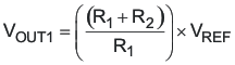
In simultaneous voltage tracking, shown in Figure 6-10, tracking signals VTRK1 and VTRK2 of two modules, POL1 and POL2, start up at the same time, and their output voltages VOUT1initial and VOUT2initial are approximately the same during initial startup. Because VTRK1 and VTRK2 are less than VREF (0.6 V, typical), Equation 12 is used. As a result, components selection must meet Equation 14.
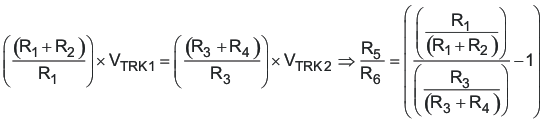
After the lower output voltage setting reaches the output-voltage VOUT1 set point, where VTRK1 increases above VREF, the output voltage of the other one (VOUT2) continues increasing until it reaches its own set point, where VTRK2 increases above VREF. At that time, Equation 13 is used. As a result, the resistor settings must meet Equation 15 and Equation 16.
Equation 14 can be simplified into Equation 17 by substituting terms from Equation 15 and Equation 16.
If 5-V VOUT2 and 2.5-V VOUT1 are required, according to Equation 15, Equation 16, and Equation 17, the selected components can be as follows:
- R5 = R6 = R4 = R2 =10 kΩ
- R1 = 3.16 kΩ
- R3 = 1.37 kΩ


In ratiometric voltage tracking as shown in Figure 6-12, the two tracking voltages, VTRK1 and VTRK2, for two modules, POL1 and POL2, are the same. Their output voltages, VOUT1 and VOUT2, are different with different voltage dividers, R2–R1 and R4–R3. VOUT1 and VOUT2 increase proportionally and reach their output voltage set points at approximately the same time.


Sequential start-up is shown in Figure 6-14. During start-up of the first module, POL1, its PGOOD1 is pulled to low. Because PGOOD1 is connected to soft-start SS2 of the second module, POL2, is not able to charge its soft-start capacitor. After output voltage VOUT1 of POL1 reaches its setting point, PGOOD1 is released. POL2 starts charging its soft-start capacitor. Finally, output voltage VOUT2 of POL2 reaches its setting point.


The TRK pin has high impedance, so it is a noise-sensitive terminal. If the tracking function is used, TI recommends a small R-C filter at the TRK pin to filter out high-frequency noise.
If the tracking function is not used, the TRK pin must be pulled up directly or through a resistor (with a value between 10 kΩ and 100 kΩ) to VDD.