SLUS719H MARCH 2007 – May 2019 TPS40192 , TPS40193
PRODUCTION DATA.
- 1 Features
- 2 Applications
- 3 Description
- 4 Revision History
- 5 Pin Configuration and Functions
- 6 Specifications
- 7 Detailed Description
-
8 Application and Implementation
- 8.1 Application Information
- 8.2
Typical Application
- 8.2.1 Design Requirements
- 8.2.2
Detailed Design Procedure
- 8.2.2.1 Selecting the Switching Frequency
- 8.2.2.2 Inductor Selection
- 8.2.2.3 Output Capacitor Selection (C8)
- 8.2.2.4 Peak Current Rating of the Inductor
- 8.2.2.5 Input Capacitor Selection (C7)
- 8.2.2.6 MOSFET Switch Selection (Q1, Q2)
- 8.2.2.7 Boot Strap Capacitor
- 8.2.2.8 Input Bypass Capacitor (C6)
- 8.2.2.9 BP5 Bypass Capacitor (C5)
- 8.2.2.10 Input Voltage Filter Resistor (R11)
- 8.2.2.11 Short Circuit Protection (R9)
- 8.2.2.12 Feedback Compensation (Modeling the Power Stage)
- 8.2.2.13 Feedback Divider (R7, R8)
- 8.2.2.14 Error Amplifier Compensation (R6, R10, C1, C2, C3)
- 8.2.3 Application Curves
- 9 Power Supply Recommendations
- 10Layout
- 11Device and Documentation Support
- 12Mechanical, Packaging, and Orderable Information
Package Options
Mechanical Data (Package|Pins)
- DRC|10
Thermal pad, mechanical data (Package|Pins)
- DRC|10
Orderable Information
7.3.5 Start-Up Sequence and Timing
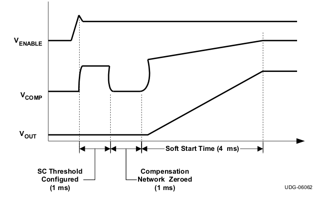
After input power is applied, the 5-V onboard regulator comes up. Once this regulator comes up, the device goes through a period where it samples the impedance at the COMP pin and determines the short circuit protection threshold voltage, by placing 400 mV on the COMP pin for approximately 1 ms. During this time, the current is measured and compared against internal thresholds to select the short circuit protection threshold. After this, the COMP pin is brought low for 1 ms. This ensures that the feedback loop is preconditioned at start-up and no sudden output rise occurs at the output of the converter when the converter is allowed to start switching. After these initial two milliseconds, the internal soft-start circuitry is engaged and the converter is allowed to start. See Figure 13.
