SLVS861F august 2008 – june 2020 TPS40210-Q1 , TPS40211-Q1
PRODUCTION DATA
- 1 Features
- 2 Applications
- 3 Description
- 4 Revision History
- 5 Pin Configuration and Functions
- 6 Specifications
-
7 Detailed Description
- 7.1 Overview
- 7.2 Functional Block Diagram
- 7.3
Feature Description
- 7.3.1 Minimum On-Time and Off-Time Considerations
- 7.3.2 Current Sense and Overcurrent
- 7.3.3 Current Sense and Subharmonic Instability
- 7.3.4 Current Sense Filtering
- 7.3.5 Soft Start
- 7.3.6 BP Regulator
- 7.3.7 Shutdown (DIS/ EN Pin)
- 7.3.8 Control Loop Considerations
- 7.3.9 Gate Drive Circuit
- 7.3.10 TPS40211-Q1
- 7.4 Device Functional Modes
-
8 Application and Implementation
- 8.1 Application Information
- 8.2
Typical Application
- 8.2.1 Design Requirements
- 8.2.2
Detailed Design Procedure
- 8.2.2.1 Duty Cycle Estimation
- 8.2.2.2 Inductor Selection
- 8.2.2.3 Rectifier Diode Selection
- 8.2.2.4 Output Capacitor Selection
- 8.2.2.5 Input Capacitor Selection
- 8.2.2.6 Current Sense and Current Limit
- 8.2.2.7 Current Sense Filter
- 8.2.2.8 Switching MOSFET Selection
- 8.2.2.9 Feedback Divider Resistors
- 8.2.2.10 Error Amplifier Compensation
- 8.2.2.11 R-C Oscillator
- 8.2.2.12 Soft-Start Capacitor
- 8.2.2.13 Regulator Bypass
- 8.2.3 Application Curves
- 9 Power Supply Recommendations
- 10Layout
- 11Device and Documentation Support
- 12Mechanical, Packaging, and Orderable Information
Package Options
Refer to the PDF data sheet for device specific package drawings
Mechanical Data (Package|Pins)
- DGQ|10
Thermal pad, mechanical data (Package|Pins)
Orderable Information
8.2.2.2 Inductor Selection
The peak-to-peak ripple is limited to 30% of the maximum output current.
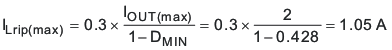
The minimum inductor size can be estimated using Equation 35.
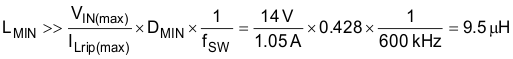
The next higher standard inductor value of 10 μH is selected. The ripple current is estimated by Equation 36.
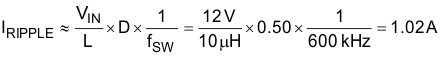
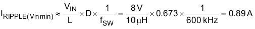
The worst-case peak-to-peak ripple current occurs at 50% duty cycle and is estimated as 1.02 A. Worst-case rms current through the inductor is approximated by Equation 38.

The worst case RMS inductor current is 6.13 Arms. The peak inductor current is estimated by Equation 39.
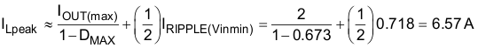
A 10-μH inductor with a minimum RMS current rating of 6.13 A and minimum saturation current rating of 6.57 A must be selected. A TDK RLF12560T-100M-7R5 7.5-A 10-μH inductor is selected.
This inductor power dissipation is estimated by Equation 40.
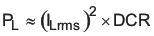
The TDK RLF12560T-100M-7R5 12.4-mΩ DCR dissipates 466 mW of power.