SLUSBT2A January 2014 – August 2014 TPS51604-Q1
PRODUCTION DATA.
- 1 Features
- 2 Applications
- 3 Description
- 4 Revision History
- 5 Pin Configuration and Functions
- 6 Specifications
- 7 Detailed Description
- 8 Layout
- 9 Device and Documentation Support
- 10Mechanical, Packaging, and Orderable Information
Package Options
Mechanical Data (Package|Pins)
- DSG|8
Thermal pad, mechanical data (Package|Pins)
- DSG|8
Orderable Information
5 Pin Configuration and Functions
DSG
8 PINS
(TOP VIEW)
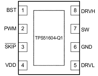
Pin Functions
| PIN | I/O(1) | DESCRIPTION | |
|---|---|---|---|
| NAME | NO. | ||
| BST | 1 | I | High-side N-channel FET bootstrap voltage input; power supply for high-side driver |
| DRVH | 8 | O | High-side N-channel gate drive output |
| DRVL | 5 | O | Synchronous low-side N-channel gate drive output |
| GND | 6 | — | Synchronous low-side N-channel gate drive return and IC reference |
| PWM | 2 | I | PWM input. A tri-state voltage on this pin turns OFF both the high-side (DRVH) and low-side drivers (DRVL) |
| SKIP | 3 | I | When SKIP is LO, the zero crossing comparator is active; the power chain enters discontinuous conduction mode when the inductor current reaches zero. When SKIP is HI, the zero crossing comparator is disabled, and the driver outputs follow the PWM input. A tri-state voltage on SKIP puts the driver into a very-low power state. |
| SW | 7 | I/O | High-side N-channel gate drive return. Also, zero-crossing sense input |
| Thermal Pad | — | Tie to system GND plane with multiple vias | |
| VDD | 4 | I | 5-V power supply input; decouple to GND with a ceramic capacitor with a value of 1 µF or greater |
(1) I = Input, O = Output