SLUSBT2A January 2014 – August 2014 TPS51604-Q1
PRODUCTION DATA.
- 1 Features
- 2 Applications
- 3 Description
- 4 Revision History
- 5 Pin Configuration and Functions
- 6 Specifications
- 7 Detailed Description
- 8 Layout
- 9 Device and Documentation Support
- 10Mechanical, Packaging, and Orderable Information
Package Options
Mechanical Data (Package|Pins)
- DSG|8
Thermal pad, mechanical data (Package|Pins)
- DSG|8
Orderable Information
6 Specifications
6.1 Absolute Maximum Ratings(1)(2)
over operating free-air temperature (unless otherwise noted)| MIN | MAX | UNIT | ||
|---|---|---|---|---|
| Input voltage | VDD | –0.3 | 6 | V |
| PWM, SKIP | –0.3 | 6 | ||
| Output voltage | BST | –0.3 | 35 | V |
| BST (transient <20 ns) | –0.3 | 38 | ||
| BST to SW; DRVH to SW | –0.3 | 6 | ||
| SW | –2 | 30 | ||
| DRVH, SW (transient <20 ns) | –5 | 38 | ||
| DRVL | –0.3 | 6 | ||
| Ground pins | GND to PAD | –0.3 | 0.3 | V |
| Operating junction temperature, TJ | –40 | 125 | °C | |
(1) Stresses beyond those listed under Absolute Maximum Ratings may cause permanent damage to the device. These are stress ratings only and functional operation of the device at these or any other conditions beyond those indicated under Recommended Operating Conditions is not implied. Exposure to absolute-maximum-rated conditions for extended periods may affect device reliability.
(2) All voltage values are with respect to the network ground terminal unless otherwise noted.
6.2 Handling Ratings
| MIN | MAX | UNIT | ||||
|---|---|---|---|---|---|---|
| Tstg | Storage temperature range | –55 | 150 | °C | ||
| V(ESD) | Electrostatic discharge | Human body model (HBM), per AEC Q100-002(1) | –2 | 2 | kV | |
| Charged device model (CDM), per AEC Q100-011 | –750 | 750 | V | |||
(1) AEC Q100-002 indicates HBM stressing is done in accordance with the ANSI/ESDA/JEDEC JS-001 specification.
6.3 Recommended Operating Conditions
Over operating free-air temperature range (unless otherwise noted)| MIN | TYP | MAX | UNIT | ||
|---|---|---|---|---|---|
| Input voltage | VDD | 4.5 | 5 | 5.5 | V |
| PWM, SKIP | –0.1 | 5.5 | |||
| Output voltage | BST | –0.1 | 34 | V | |
| BST to SW; DRVH to SW | –0.1 | 5.5 | |||
| SW | –1 | 28 | |||
| DRVL | –0.1 | 5.5 | |||
| Ground pins | GND to PAD | –0.1 | 0.1 | V | |
| Operating junction temperature, TJ | –40 | 125 | °C | ||
6.4 Thermal Information
| THERMAL METRIC(1) | TPS51604-Q1 | UNIT | |
|---|---|---|---|
| WSON (DSG) (8 PINS) |
|||
| RθJA | Junction-to-ambient thermal resistance | 63.1 | °C/W |
| RθJC(top) | Junction-to-case (top) thermal resistance | 74.1 | |
| RθJB | Junction-to-board thermal resistance | 34.3 | |
| ψJT | Junction-to-top characterization parameter | 2.0 | |
| ψJB | Junction-to-board characterization parameter | 34.9 | |
| RθJC(bot) | Junction-to-case (bottom) thermal resistance | 11.7 | |
(1) For more information about traditional and new thermal metrics, see the IC Package Thermal Metrics application report, SPRA953.
6.5 Electrical Characteristics
These specifications apply for TJ = –40°C to 125°C and VDD = 5 V unless otherwise specified.| PARAMETER | TEST CONDITIONS | MIN | TYP | MAX | UNIT | |
|---|---|---|---|---|---|---|
| VDD INPUT SUPPLY | ||||||
| ICC | Supply current (operating) | VSKIP = VVDD or VSKIP = 0 V, PWM = High | 160 | 600 | µA | |
| VSKIP = VVDD or VSKIP = 0 V, PWM = Low | 250 | |||||
| VSKIP = VVDD or VSKIP = 0 V, PWM = Float | 130 | |||||
| VSKIP = Float | 8 | |||||
| VDD UNDERVOLTAGE LOCKOUT (UVLO) | ||||||
| VUVLO | UVLO threshold | Rising threshold | 4.15 | V | ||
| Falling threshold | 3.7 | |||||
| VUVHYS | UVLO hysteresis | 0.2 | V | |||
| PWM AND SKIP I/O SPECIFICATIONS | ||||||
| RI | Input impedance | Pullup to VDD | 1.7 | MΩ | ||
| Pulldown (to GND) | 800 | kΩ | ||||
| VIL | Low-level input voltage | 0.6 | V | |||
| VIH | High-level input voltage | 2.65 | ||||
| VIHH | Hysteresis | 0.2 | ||||
| VTS | Tri-state voltage | 1.3 | 2.0 | |||
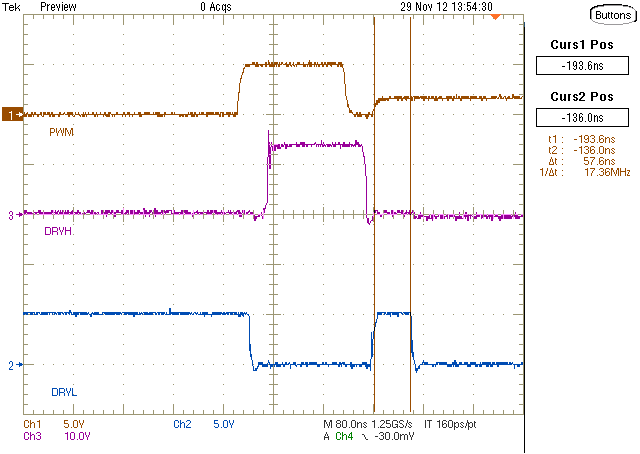
| tTHOLD(off1) | Tri-state activation time (falling) PWM | 60 | ns | |||
| tTHOLD(off2) | Tri-state activation time (rising) PWM | 60 | ||||
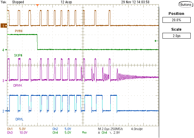
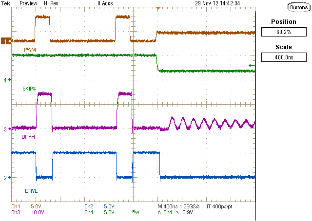
| tTSKF | Tri-state activation time (falling) SKIP | 1 | µs | |||
| tTSKR | Tri-state activation time (rising) SKIP | 1 | ||||
| t3RD(PWM) | Tri-state exit time PWM | 100 | ns | |||
| t3RD(SKIP) | Tri-state exit time SKIP | 50 | µs | |||
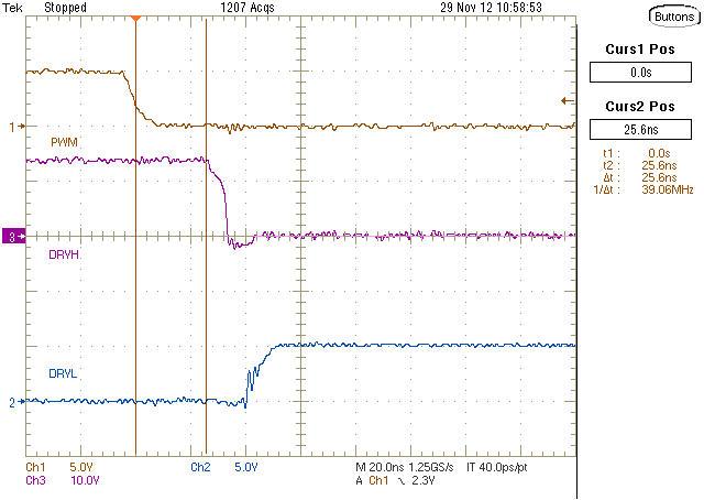
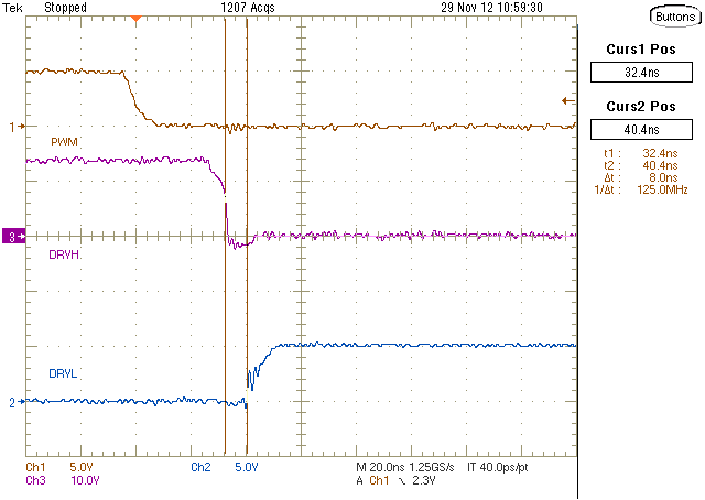
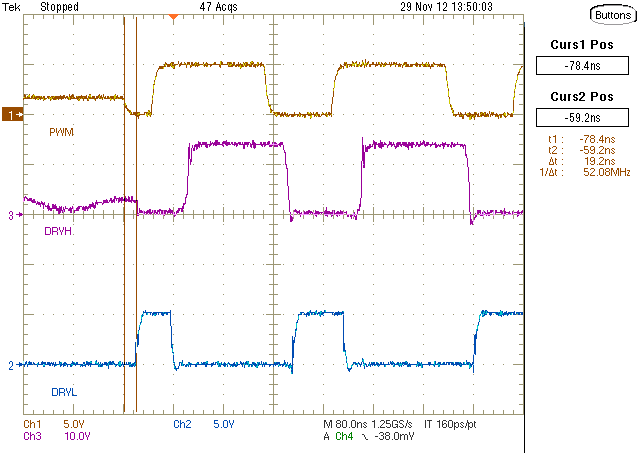
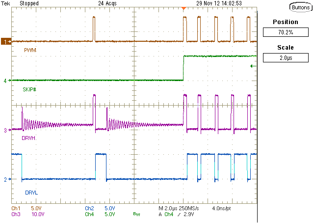
| HIGH-SIDE GATE DRIVER (DRVH) | ||||||
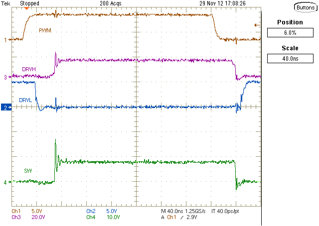
| tR(DRVH) | Rise time | DRVH rising, CDRVH = 3.3 nF; 20% to 80% | 30 | ns | ||
| tRPD(DRVH) | Rise time propogation delay | CDRVH = 3.3 nF | 40 | ns | ||
| RSRC | Source resistance | Source resistance, (VBST– VSW) = 5 V, high state, (VBST – VDRVH) = 0.1 V | 4 | 8 | Ω | |
| tF(DRVH) | Fall time | DRVH falling, CDRVH = 3.3 nF | 8 | ns | ||
| tFPD(DRVH) | Fall-time propagation delay | CDRVH = 3.3 nF | 25 | ns | ||
| RSNK | Sink resistance | Sink resistance, (VBST – VSW) forced to 5 V, low state (VDRVH – VSW) = 0.1 V | 0.5 | 1.6 | Ω | |
| RDRVH | DRVH to SW resistance(1) | 100 | kΩ | |||
| LOW-SIDE GATE DRIVER (DRVL) | ||||||
| tR(DRVL) | Rise time | DRVL rising, CDRVL = 3.3 nF; 20% to 80% | 15 | ns | ||
| tRPD(DRVL) | Rise time propagation delay | CDRVL = 3.3 nF | 35 | ns | ||
| RSRC | Source resistance | Source resistance, (VVDD–GND) = 5 V, high state, (VVDD – VDRVL) = 0.1 V | 1.5 | 3 | Ω | |
| tF(DRVL) | Fall time | DRVL falling, CDRVL = 3.3 nF | 10 | ns | ||
| tFPD(DRVL) | Fall-time propagation delay | CDRVL= 3.3 nF | 15 | ns | ||
| RSNK | Sink resistance | Sink resistance, (VVDD– GND) = 5 V, low state, (VDRVL – GND) = 0.1 V | 0.4 | 1.6 | Ω | |
| RDRVL | DRVL to GND resistance(1) | 100 | kΩ | |||
| GATE DRIVER DEAD-TIME | ||||||
| tR(DT) | Rising edge | 0 | 20 | 35 | ns | |
| tF(DT) | Falling edge | 0 | 10 | 25 | ns | |
| ZERO CROSSING COMPARATOR | ||||||
| VZX | Zero crossing offset | SW voltage rising | –2.25 | 0 | 2.00 | mV |
| BOOTSTRAP SWITCH | ||||||
| VFBST | Forward voltage | IF = 10 mA | 120 | 240 | mV | |
| IRLEAK | Reverse leakage | (VBST – VVDD) = 25 V | 2 | µA | ||
| RDS(on) | On-resistance | 12 | 24 | Ω | ||
(1) Specified by design. Not production tested.
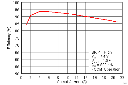
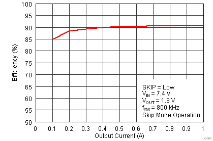
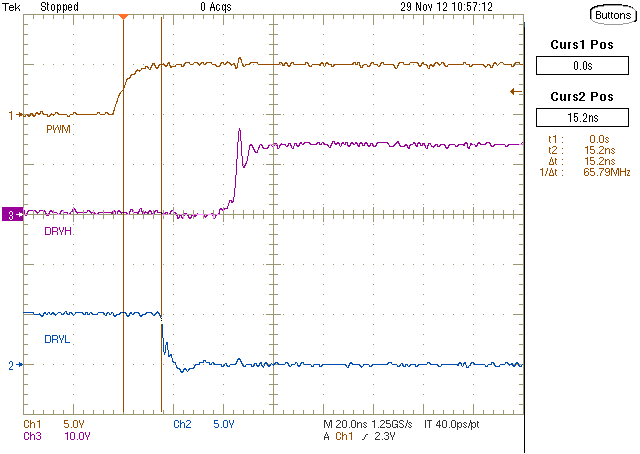
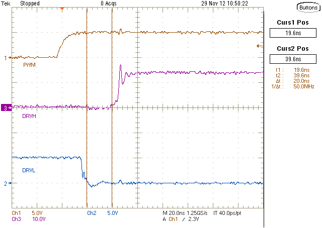
6.6 Typical Characteristics
6.7 Typical Power Block MOSFET Characteristics
Power block MOSFET: CSD87330 (SLPS284), Inductor: 0.22 µF, 1.1-mΩ DCR