SLUSAE6B December 2010 – November 2023 TPS53315
PRODUCTION DATA
- 1
- 1 Features
- 2 Applications
- 3 Description
- 4 Pin Configuration and Functions
- 5 Specifications
-
6 Detailed Description
- 6.1 Overview
- 6.2 Functional Block Diagram
- 6.3
Feature Description
- 6.3.1 D-CAP™ Integrated Circuit with Adaptive On-Time
- 6.3.2 Small Signal Model
- 6.3.3 Ramp Signal
- 6.3.4 Auto-Skip Eco-mode Light Load Operation
- 6.3.5 Adaptive Zero Crossing
- 6.3.6 Forced Continuous Conduction Mode
- 6.3.7 Power Good
- 6.3.8 Current Sense and Overcurrent Protection
- 6.3.9 Overvoltage and Undervoltage Protection
- 6.3.10 UVLO Protection
- 6.3.11 Thermal Shutdown
- 6.4 Device Functional Modes
-
7 Application and Implementation
- 7.1 Application Information
- 7.2
Typical Application
- 7.2.1
Typical Application Circuit Diagram
- 7.2.1.1 Design Requirements
- 7.2.1.2
Detailed Design Procedure
- 7.2.1.2.1 Step 1: Select Operation Mode and Soft-Start Time
- 7.2.1.2.2 Step 2: Select Switching Frequency
- 7.2.1.2.3 Step 3: Select the Inductance
- 7.2.1.2.4 Step 4: Select Output Capacitors
- 7.2.1.2.5 Step 5: Determine the Voltage-Divider Resistance (R1 and R2)
- 7.2.1.2.6 Step 6: Select the Overcurrent Resistance (RTRIP)
- 7.2.1.3 Application Curves
- 7.2.2 Typical Application Circuit Diagram With Ceramic Output Capacitors
- 7.2.1
Typical Application Circuit Diagram
- 7.3 Power Supply Recommendations
- 7.4 Layout
- 8 Device and Documentation Support
- 9 Revision History
- 10Mechanical, Packaging, and Orderable Information
Package Options
Mechanical Data (Package|Pins)
- RGF|40
Thermal pad, mechanical data (Package|Pins)
- RGF|40
Orderable Information
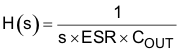
6.3.2 Small Signal Model
From small-signal loop analysis, a buck converter using D-CAP integrated circuit can be simplified as shown in Figure 6-3.
 Figure 6-3 Simplified Modulator Model
The output voltage is compared with the internal reference voltage (ramp signal is ignored here for simplicity). The PWM comparator determines the timing to turn on the high-side MOSFET. The gain and speed of the comparator can be assumed high enough to keep the voltage at the beginning of each on-cycle substantially constant.
For the loop stability, the 0 dB frequency, ƒ0, defined in Equation 2 must be lower than ¼ of the switching frequency.
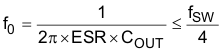
According to Equation 2, the loop stability of D-CAP integrated circuit modulator is mainly determined by the capacitor chemistry. For example, specialty polymer capacitors (SP-CAP) have COUT on the order of several 100 µF and ESR in range of 10 mΩ. These makes ƒ0 on the order of 100 kHz or less and the loop is stable. However, ceramic capacitors have an ƒ0 at more than 700 kHz, and need special care when used with this modulator. An application circuit using ceramic capacitors is described in Section 7.2.2.3 section.