SLUSAK4D June   2011  – July 2015 TPS53317

PRODUCTION DATA.  

  1. Features
  2. Applications
  3. Description
  4. Revision History
  5. Pin Configuration and Functions
  6. Specifications
    1. 6.1 Absolute Maximum Ratings
    2. 6.2 ESD Ratings
    3. 6.3 Recommended Operating Conditions
    4. 6.4 Thermal Information
    5. 6.5 Electrical Characteristics
    6. 6.6 Typical Characteristics
  7. Detailed Description
    1. 7.1 Overview
    2. 7.2 Functional Block Diagram
    3. 7.3 Feature Description
      1. 7.3.1 PWM Operation
      2. 7.3.2 PWM Frequency and Adaptive On-Time Control
      3. 7.3.3 Light-Load Power Saving Features
      4. 7.3.4 Power Sequences
        1. 7.3.4.1 Non-Tracking Startup
        2. 7.3.4.2 Tracking Startup
      5. 7.3.5 Protection Features
        1. 7.3.5.1 5-V Undervoltage Protection (UVLO)
        2. 7.3.5.2 Power Good Signals
        3. 7.3.5.3 Output Overvoltage Protection (OVP)
        4. 7.3.5.4 Output Undervoltage Protection (UVP)
        5. 7.3.5.5 Overcurrent Protection
          1. 7.3.5.5.1 Overcurrent Limit
          2. 7.3.5.5.2 Negative OCL
      6. 7.3.6 Thermal Protection
    4. 7.4 Device Functional Modes
      1. 7.4.1 Non-Droop Configuration
      2. 7.4.2 Droop Configuration
  8. Application and Implementation
    1. 8.1 Application Information
    2. 8.2 Typical Applications
      1. 8.2.1 DDR4 SDRAM Application
        1. 8.2.1.1 Design Requirements
        2. 8.2.1.2 Detailed Design Procedure
          1. 8.2.1.2.1 Step 1. Determine Configuration
          2. 8.2.1.2.2 Step 2. Select Inductor
          3. 8.2.1.2.3 Step 3. Determine Output Capacitance
          4. 8.2.1.2.4 Step 4. Input Capacitance
          5. 8.2.1.2.5 Step 5. Compensation Network
          6. 8.2.1.2.6 Peripheral Component Selection
        3. 8.2.1.3 Application Curves
      2. 8.2.2 DDR3 SDRAM Application
        1. 8.2.2.1 Design Requirements
      3. 8.2.3 Non-Tracking Point-of-Load (POL) Application
        1. 8.2.3.1 Design Requirements
        2. 8.2.3.2 Application Curves
  9. Power Supply Recommendations
  10. 10Layout
    1. 10.1 Layout Guidelines
    2. 10.2 Layout Example
  11. 11Device and Documentation Support
    1. 11.1 Community Resources
    2. 11.2 Trademarks
    3. 11.3 Electrostatic Discharge Caution
    4. 11.4 Glossary
  12. 12Mechanical, Packaging, and Orderable Information

Package Options

Mechanical Data (Package|Pins)
Thermal pad, mechanical data (Package|Pins)
Orderable Information

10 Layout

10.1 Layout Guidelines

Stable power supply operation depends on proper layout. Follow these guidelines for an optimized PCB layout.

  • Connect PGND pins to the thermal pad underneath the device. Use four vias to connect the thermal pad to internal ground planes.
  • Place VIN, V5IN and VREF decoupling capacitors as close to the device as possible.
  • Use wide traces for the VIN, PGND and SW pins. These nodes carry high current and also serve as heat sinks.
  • Place feedback and compensation components as close to the device as possible.
  • Place COMP and VOUT analog signal traces away from noisy signals (SW, BST).
  • The GND pin should connect to the PGND in only one place, through a via or a 0-Ω resistor.

10.2 Layout Example
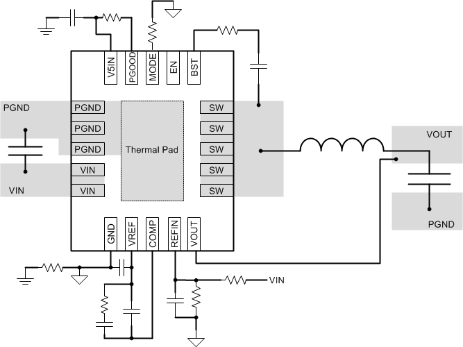
TPS53317 layout_slusak4.gifFigure 41. TPS53317 Board Layout