SLVSB10F July 2012 – November 2020 TPS54020
PRODUCTION DATA
- 1 Features
- 2 Applications
- 3 Description
- 4 Revision History
- 5 Description (Continued)
- 6 Pin Configuration and Functions
- 7 Specifications
-
8 Detailed Description
- 8.1 Overview
- 8.2 Functional Block Diagram
- 8.3
Feature Description
- 8.3.1 Fixed Frequency PWM Control
- 8.3.2 Input Voltage and Power Input Voltage Pins (VIN and PVIN)
- 8.3.3 Voltage Reference (VREF)
- 8.3.4 Adjusting the Output Voltage
- 8.3.5 Safe Start-up into Prebiased Outputs
- 8.3.6 Error Amplifier
- 8.3.7 Slope Compensation
- 8.3.8 Enable and Adjusting Undervoltage Lockout
- 8.3.9 Adjustable Switching Frequency and Synchronization (RT/CLK)
- 8.3.10 Soft-Start (SS) Sequence
- 8.3.11 Power Good (PWRGD)
- 8.3.12 Bootstrap Voltage (BOOT) and Low Dropout Operation
- 8.3.13 Sequencing (SS)
- 8.3.14 Output Overvoltage Protection (OVP)
- 8.3.15 Overcurrent Protection
- 8.3.16 Thermal Shutdown
- 8.4 Device Functional Modes
-
9 Application and Implementation
- 9.1 Application Information
- 9.2
Typical Application
- 9.2.1 Design Requirements
- 9.2.2
Detailed Design Procedure
- 9.2.2.1 Custom Design With WEBENCH® Tools
- 9.2.2.2 Operating Frequency
- 9.2.2.3 Output Inductor Selection
- 9.2.2.4 Output Capacitor Selection
- 9.2.2.5 Input Capacitor Selection
- 9.2.2.6 Soft-Start Capacitor Selection
- 9.2.2.7 Bootstrap Capacitor Selection
- 9.2.2.8 Undervoltage Lockout Set Point
- 9.2.2.9 Output Voltage Feedback Resistor Selection
- 9.2.2.10 Compensation Component Selection
- 9.2.3 Application Curves
- 10Power Supply Recommendations
- 11Layout
- 12Device and Documentation Support
- 13Mechanical, Packaging, and Orderable Information
Package Options
Mechanical Data (Package|Pins)
- RUW|15
Thermal pad, mechanical data (Package|Pins)
- RUW|15
Orderable Information
9.2.2.4.2 Output Voltage Ripple
The output voltage ripple is the second criteria. Equation 23 calculates the minimum output capacitance required to meet the output voltage ripple specification.
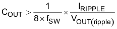
where
- fSW is the switching frequency
- VRIPPLE is the maximum allowable output voltage ripple
- IRIPPLE is the inductor ripple current.
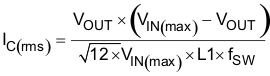
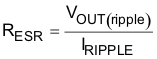
In this case, the maximum output voltage ripple is 10 mV. Under this requirement, the minimum output capacitance for ripple (as calculated in Equation 24) yields 80.5 µF. Equation 24 calculates the maximum ESR an output capacitor can have to meet the output voltage ripple specification. Equation 24 indicates the ESR should be less than 3 mΩ, and this is the requirement when the impedance of the output capacitance is dominated by ESR, such as with an electrolytic capacitor. However, because the output voltage ripple is a combination of capacitive ripple and resistive ripple, the ESR must be much lower than this result when the capacitance is purely ceramic. This is because the lower capacitance values obtained with ceramic capacitors will result in a larger capacitive ripple component of the total ripple.
Additional capacitance de-ratings for aging, temperature, and DC bias should be factored in, which increases the minimum required capacitance value. For this design example, three 100-μF, 6.3-V, X5R, ceramic capacitors with 2 mΩ each of ESR were selected. Capacitors generally have limits to the amount of ripple current they can handle without failing or producing excess heat. An output capacitor that can support the inductor ripple current must be specified. Some capacitor data sheets specify the RMS (root mean square) value of the maximum ripple current. Equation 25 can be used to calculate the RMS ripple current the output capacitor needs to support. For this application, Equation 25 yields 929 mA.