SLVS416C February 2002 – January 2015 TPS54311 , TPS54312 , TPS54313 , TPS54314 , TPS54315 , TPS54316
PRODUCTION DATA.
- 1 Features
- 2 Applications
- 3 Description
- 4 Revision History
- 5 Pin Configuration and Functions
- 6 Specifications
-
7 Detailed Description
- 7.1 Overview
- 7.2 Functional Block Diagram
- 7.3
Feature Description
- 7.3.1 Undervoltage Lock Out (UVLO)
- 7.3.2 Slow-Start/Enable (SS/ENA)
- 7.3.3 VBIAS Regulator (VBIAS)
- 7.3.4 Voltage Reference
- 7.3.5 Oscillator and PWM Ramp
- 7.3.6 Error Amplifier
- 7.3.7 PWM Control
- 7.3.8 Dead-Time Control and MOSFET Drivers
- 7.3.9 Overcurrent Protection
- 7.3.10 Thermal Shutdown
- 7.3.11 Powergood (PWRGD)
- 7.4 Device Functional Modes
- 8 Application and Implementation
- 9 Power Supply Recommendations
- 10Layout
- 11Device and Documentation Support
- 12Mechanical, Packaging, and Orderable Information
Package Options
Mechanical Data (Package|Pins)
- PWP|20
Thermal pad, mechanical data (Package|Pins)
- PWP|20
Orderable Information
7 Detailed Description
7.1 Overview
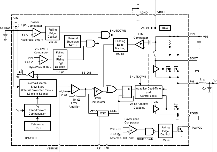
As members of the SWIFT™ family of DC - DC regulators, the TPS54311, TPS54312, TPS54313, TPS54314, TPS54315, and TPS54316 low-input-voltage high-outputcurrent synchronous-buck PWM converters integrate all required active components. Included on the substrate with the listed features are a true, high performance, voltage error amplifier that provides high performance under transient conditions; an undervoltage-lockout circuit to prevent start-up until the input voltage reaches 3 V; an internally and externally set slow-start circuit to limit in-rush currents; and a powergood output useful for processor/logic reset, fault signaling, and supply sequencing.
7.2 Functional Block Diagram
7.3 Feature Description
7.3.1 Undervoltage Lock Out (UVLO)
The TPS5431x incorporates an UVLO circuit to keep the device disabled when the input voltage (VIN) is insufficient. During power up, internal circuits are held inactive until VIN exceeds the nominal UVLO threshold voltage of 2.95 V. Once the UVLO start threshold is reached, device start-up begins. The device operates until VIN falls below the nominal UVLO stop threshold of 2.8 V. Hysteresis in the UVLO comparator, and a 2.5-µs rising and falling edge deglitch circuit reduce the likelihood of shutting the device down due to noise on VIN.
7.3.2 Slow-Start/Enable (SS/ENA)
The slow-start/enable pin provides two functions; first, the pin acts as an enable (shutdown) control by keeping the device turned off until the voltage exceeds the start threshold voltage of approximately 1.2 V. When SS/ENA exceeds the enable threshold, device start up begins. The reference voltage fed to the error amplifier is linearly ramped up from 0 V to 0.891 V in 3.35 ms. Similarly, the converter output voltage reaches regulation in approximately 3.35 ms. Voltage hysteresis and a 2.5-µs falling edge deglitch circuit reduce the likelihood of triggering the enable due to noise.
Table 1. Device Startup Times
| DEVICE | OUTPUT VOLTAGE | SLOW-START |
|---|---|---|
| TPS54311 | 0.9 V | 3.3 ms |
| TPS54312 | 1.2 V | 4.5 ms |
| TPS54313 | 1.5 V | 5.6 ms |
| TPS54314 | 1.8 V | 3.3 ms |
| TPS54315 | 2.5 V | 4.7 ms |
| TPS54316 | 3.3 V | 6.1 ms |
The second function of the SS/ENA pin provides an external means of extending the slow-start time with a low-value capacitor connected between SS/ENA and AGND. Adding a capacitor to the SS/ENA pin has two effects on start-up. First, a delay occurs between release of the SS/ENA pin and start up of the output. The delay is proportional to the slow-start capacitor value and lasts until the SS/ENA pin reaches the enable threshold. The start-up delay is approximately:
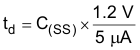
Second, as the output becomes active, a brief ramp up at the internal slow-start rate may be observed before the externally set slow-start rate takes control and the output rises at a rate proportional to the slow-start capacitor. The slow-start time set by the capacitor is approximately:
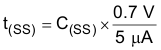
The actual slow-start time is likely to be less than the above approximation due to the brief ramp up at the internal rate
7.3.3 VBIAS Regulator (VBIAS)
The VBIAS regulator provides internal analog and digital blocks with a stable supply voltage over variations in junction temperature and input voltage. A high quality, low-ESR, ceramic bypass capacitor is required on the VBIAS pin. X7R or X5R grade dielectrics are recommended because their values are more stable over temperature. The bypass capacitor should be placed close to the VBIAS pin and returned to AGND. External loading on VBIAS is allowed, with the caution that internal circuits require a minimum VBIAS of 2.70 V, and external loads on VBIAS with ac or digital switching noise may degrade performance. The VBIAS pin may be useful as a reference voltage for external circuits.
7.3.4 Voltage Reference
The voltage reference system produces a precise Vref signal by scaling the output of a temperature stable bandgap circuit. During manufacture, the bandgap and scaling circuits are trimmed to produce 0.891 V at the output of the error amplifier, with the amplifier connected as a voltage follower. The trim procedure adds to the high precision regulation of the TPS5431x, since it cancels offset errors in the scale and error amplifier circuits.
7.3.5 Oscillator and PWM Ramp
The oscillator frequency can be set to internally fixed values of 350 kHz or 550 kHz using the FSEL pin as a static digital input. If a different frequency of operation is required for the application, the oscillator frequency can be externally adjusted from 280 kHz to 700 kHz by connecting a resistor to the RT pin to ground and floating the FSEL pin. The switching frequency is approximated by the following equation, where R is the resistance from RT to AGND:

Table 2. Summary of the Frequency Selection Configurations
| SWITCHING FREQUENCY | FSEL PIN | RT PIN |
|---|---|---|
| 350 kHz, internally set | Float or AGND | Float |
| 550 kHz, internally set | ≥2.5 V | Float |
| Externally set 280 kHz to 700 kHz | Float | R = 68 kΩ to 180 kΩ |
7.3.6 Error Amplifier
The high performance, wide bandwidth, voltage error amplifier is gain limited to provide internal compensation of the control loop. The user is given limited flexibility in choosing output L and C filter components. Inductance values of 4.7 µH to 10 µH are typical and available from several vendors. The resulting designs exhibit good noise and ripple characteristics, along with exceptional transient response. Transient recovery times are typically in the range of 10 to 20 µs.
7.3.7 PWM Control
Signals from the error amplifier output, oscillator, and current limit circuit are processed by the PWM control logic. Referring to the internal block diagram, the control logic includes the PWM comparator, OR gate, PWM latch, and portions of the adaptive dead-time and control logic block. During steady-state operation below the current limit threshold, the PWM comparator output and oscillator pulse train alternately reset and set the PWM latch. Once the PWM latch is set, the low-side FET remains on for a minimum duration set by the oscillator pulse duration. During this period, the PWM ramp discharges rapidly to its valley voltage. When the ramp begins to charge back up, the low-side FET turns off and high-side FET turns on. As the PWM ramp voltage exceeds the error amplifier output voltage, the PWM comparator resets the latch, thus turning off the high-side FET and turning on the low-side FET. The low-side FET remains on until the next oscillator pulse discharges the PWM ramp
During transient conditions, the error amplifier output could be below the PWM ramp valley voltage or above the PWM peak voltage. If the error amplifier is high, the PWM latch is never reset and the high-side FET remains on until the oscillator pulse signals the control logic to turn the high-side FET off and the low-side FET on. The device operates at its maximum duty cycle until the output voltage rises to the regulation set-point, setting VSENSE to approximately the same voltage as Vref. If the error amplifier output is low, the PWM latch is continually reset and the high-side FET does not turn on. The low-side FET remains on until the VSENSE voltage decreases to a range that allows the PWM comparator to change states. The TPS5431x is capable of sinking current continuously until the output reaches the regulation set-point.
If the current limit comparator trips for longer than 100 ns, the PWM latch resets before the PWM ramp exceeds the error amplifier output. The high-side FET turns off and low-side FET turns on to decrease the energy in the output inductor and consequently the output current. This process is repeated each cycle in which the current limit comparator is tripped.
7.3.8 Dead-Time Control and MOSFET Drivers
Adaptive dead-time control prevents shoot-through current from flowing in both N-channel power MOSFETs during the switching transitions by actively controlling the turnon times of the MOSFET drivers. The high-side driver does not turn on until the voltage at the gate of the low-side FET is below 2 V. The high-side and low-side drivers are designed with 300 mA source and sink capability to quickly drive the power MOSFETs gates. The low-side driver is supplied from VIN, while the high-side drive is supplied from the BOOT pin. A bootstrap circuit uses an external BOOT capacitor and internal 2.5-Ω bootstrap switch connected between the VIN and BOOT pins. The integrated bootstrap switch improves drive efficiency and reduces external component count.
7.3.9 Overcurrent Protection
The cycle by cycle current limiting is achieved by sensing the current flowing through the high-side MOSFET and differential amplifier and comparing it to the preset overcurrent threshold. The high-side MOSFET is turned off within 200 ns of reaching the current limit threshold. A 100-ns leading edge blanking circuit prevents false tripping of the current limit. Current limit detection occurs only when current flows from VIN to PH when sourcing current to the output filter. Load protection during current sink operation is provided by thermal shutdown.
7.3.10 Thermal Shutdown
The device uses the thermal shutdown to turn off the power MOSFETs and disable the controller if the junction temperature exceeds 150°C. The device is released from shutdown when the junction temperature decreases to 10°C below the thermal shutdown trip point and starts up under control of the slow-start circuit. Thermal shutdown provides protection when an overload condition is sustained for several milliseconds. With a persistent fault condition, the device cycles continuously; starting up by control of the soft-start circuit, heating up due to the fault, and then shutting down upon reaching the thermal shutdown point.
7.3.11 Powergood (PWRGD)
The powergood circuit monitors for undervoltage conditions on VSENSE. If the voltage on VSENSE is 10% below the reference voltage, the open-drain PWRGD output is pulled low. PWRGD is also pulled low if VIN is less than the UVLO threshold, or SS/ENA is low, or thermal shutdown is asserted. When VIN = UVLO threshold, SS/ENA = enable threshold, and VSENSE > 90% of Vref, the open-drain output of the PWRGD pin is high. A hysteresis voltage equal to 3% of Vref and a 35-µs falling edge deglitch circuit prevent tripping of the powergood comparator due to high frequency noise.
7.4 Device Functional Modes
7.4.1 Continuous Conduction Mode
The TPS5431x devices operate in continuous conduction mode, i.e. the low-side MOSFET runs fully complimentary to the high-side MOSFET regardless of output current.
7.4.2 Switching Frequency Selection/Synchronization
Depending on the configuration of the RT and SYNC pins, the TPS5431x can be configured to switch at 350 kHz, or 550 kHz without external components, or any frequency between 280 kHz and 700 kHz as configured by a resistor from the RT pin to ground. The TPS54310 can also be synchronized to an external clock using the SYNC pin. See Table 2 for more information.