SLVS416C February 2002 – January 2015 TPS54311 , TPS54312 , TPS54313 , TPS54314 , TPS54315 , TPS54316
PRODUCTION DATA.
- 1 Features
- 2 Applications
- 3 Description
- 4 Revision History
- 5 Pin Configuration and Functions
- 6 Specifications
-
7 Detailed Description
- 7.1 Overview
- 7.2 Functional Block Diagram
- 7.3
Feature Description
- 7.3.1 Undervoltage Lock Out (UVLO)
- 7.3.2 Slow-Start/Enable (SS/ENA)
- 7.3.3 VBIAS Regulator (VBIAS)
- 7.3.4 Voltage Reference
- 7.3.5 Oscillator and PWM Ramp
- 7.3.6 Error Amplifier
- 7.3.7 PWM Control
- 7.3.8 Dead-Time Control and MOSFET Drivers
- 7.3.9 Overcurrent Protection
- 7.3.10 Thermal Shutdown
- 7.3.11 Powergood (PWRGD)
- 7.4 Device Functional Modes
- 8 Application and Implementation
- 9 Power Supply Recommendations
- 10Layout
- 11Device and Documentation Support
- 12Mechanical, Packaging, and Orderable Information
Package Options
Mechanical Data (Package|Pins)
- PWP|20
Thermal pad, mechanical data (Package|Pins)
- PWP|20
Orderable Information
5 Pin Configuration and Functions
PWP Package
20-Pin HTSSOP
Top View
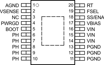
NC – No internal connection
Pin Functions
| PIN | DESCRIPTION | |
|---|---|---|
| NAME | NO. | |
| AGND | 1 | Analog ground. Return for compensation network/output divider, slow-start capacitor, VBIAS capacitor, RT resistor and FSEL pin. Make PowerPAD connection to AGND. |
| BOOT | 5 | Bootstrap input. 0.022-µF to 0.1-µF low-ESR capacitor connected from BOOT to PH generates floating drive for the high-side FET driver. |
| FSEL | 19 | Frequency select input. Provides logic input to select between two internally set switching frequencies. |
| NC | 3 | No connection |
| PGND | 11−13 | Power ground. High current return for the low-side driver and power MOSFET. Connect PGND with large copper areas to the input and output supply returns, and negative terminals of the input and output capacitors. |
| PH | 6−10 | Phase input/output. Junction of the internal high and low-side power MOSFETs, and output inductor. |
| PWRGD | 4 | Powergood open-drain output. Hi-Z when VSENSE ≥ 90% Vref, otherwise PWRGD is low. Note that output is low when SS/ENA is low or internal shutdown signal active. |
| RT | 20 | Frequency setting resistor input. Connect a resistor from RT to AGND to set the switching frequency, fs. |
| SS/ENA | 18 | Slow-start/enable input/output. Dual function pin which provides logic input to enable/disable device operation and capacitor input to externally set the start-up time. |
| VBIAS | 17 | Internal bias regulator output. Supplies regulated voltage to internal circuitry. Bypass VBIAS pin to AGND pin with a high quality, low ESR 0.1-µF to 1.0-µF ceramic capacitor. |
| VIN | 14−16 | Input supply for the power MOSFET switches and internal bias regulator. Bypass VIN pins to PGND pins close to device package with a high quality, low ESR 1-µF to 10-µF ceramic capacitor. |
| VSENSE | 2 | Error amplifier inverting input. Connect directly to output voltage sense point. |