SLVS757E March 2007 – July 2022 TPS5450
PRODUCTION DATA
- 1 Features
- 2 Applications
- 3 Description
- 4 Revision History
- 5 Pin Configuration and Functions
- 6 Specifications
-
7 Detailed Description
- 7.1 Overview
- 7.2 Functional Block Diagram
- 7.3
Feature Description
- 7.3.1 Oscillator Frequency
- 7.3.2 Voltage Reference
- 7.3.3 Enable (ENA) and Internal Slow-Start
- 7.3.4 Undervoltage Lockout (UVLO)
- 7.3.5 Boost Capacitor (BOOT)
- 7.3.6 Output Feedback (VSENSE) and Internal Compensation
- 7.3.7 Voltage Feed-Forward
- 7.3.8 Pulse-Width-Modulation (PWM) Control
- 7.3.9 Overcurrent Limiting
- 7.3.10 Overvoltage Protection
- 7.3.11 Thermal Shutdown
- 7.4 Device Functional Modes
-
8 Application and Implementation
- 8.1 Application Information
- 8.2
Typical Application
- 8.2.1 Design Requirements
- 8.2.2 Detailed Design Procedure
- 8.2.3 Application Curves
- 9 Power Supply Recommendations
- 10Layout
- 11Device and Documentation Support
- 12Mechanical, Packaging, and Orderable Information
Package Options
Refer to the PDF data sheet for device specific package drawings
Mechanical Data (Package|Pins)
- DDA|8
Thermal pad, mechanical data (Package|Pins)
- DDA|8
Orderable Information
8.2.2.3 Input Capacitors
The TPS5450 requires an input decoupling capacitor and, depending on the application, a bulk input capacitor. The minimum recommended decoupling capacitance is 4.7 μF. A high-quality ceramic type X5R or X7R is required. For some applications, a smaller value decoupling capacitor may be used, so long as the input voltage and current ripple ratings are not exceeded. The voltage rating must be greater than the maximum input voltage, including ripple.
This input ripple voltage can be approximated by Equation 3:
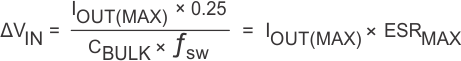
where
- IOUT(MAX) is the maximum load current
- fSW is the switching frequency
- CIN is the input capacitor value
- ESRMAX is the maximum series resistance of the input capacitor
For this design, the input capacitance consists of two 4.7-μF capacitors, C1 and C4, in parallel. An additional high frequency bypass capacitor, C5 is also used.
The maximum RMS ripple current also needs to be checked. For worst case conditions, this can be approximated by Equation 4:
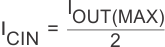
In this case the input ripple voltage would be 281 mV and the RMS ripple current would be 2.5 A. The maximum voltage across the input capacitors would be VIN max plus delta VIN/2. The chosen input decoupling capacitor is rated for 50 V and the ripple current capacity is greater than 2.5 A each, providing ample margin. It is very important that the maximum ratings for voltage and current are not exceeded under any circumstance.
Additionally some bulk capacitance may be needed, especially if the TPS5450 circuit is not located within about 2 inches from the input voltage source. The value for this capacitor is not critical but it also should be rated to handle the maximum input voltage including ripple voltage and should filter the output so that input ripple voltage is acceptable.