SLVSBO1G July 2013 – June 2021 TPS54561
PRODUCTION DATA
- 1 Features
- 2 Applications
- 3 Description
- 4 Revision History
- 5 Pin Configuration and Functions
- 6 Specifications
-
7 Detailed Description
- 7.1 Overview
- 7.2 Functional Block Diagram
- 7.3
Feature Description
- 7.3.1 Fixed Frequency PWM Control
- 7.3.2 Slope Compensation Output Current
- 7.3.3 Pulse Skip Eco-mode
- 7.3.4 Low Dropout Operation and Bootstrap Voltage (BOOT)
- 7.3.5 Error Amplifier
- 7.3.6 Adjusting the Output Voltage
- 7.3.7 Enable and Adjusting Undervoltage Lockout
- 7.3.8 Soft Start/Tracking Pin (SS/TR)
- 7.3.9 Sequencing
- 7.3.10 Constant Switching Frequency and Timing Resistor (RT/CLK) Pin)
- 7.3.11 Maximum Switching Frequency
- 7.3.12 Synchronization to RT/CLK Pin
- 7.3.13 Accurate Current Limit Operation
- 7.3.14 Power Good (PWRGD Pin)
- 7.3.15 Overvoltage Protection
- 7.3.16 Thermal Shutdown
- 7.3.17 Small Signal Model for Loop Response
- 7.3.18 Simple Small Signal Model for Peak Current Mode Control
- 7.3.19 Small Signal Model for Frequency Compensation
- 7.4 Device Functional Modes
-
8 Application and Implementation
- 8.1 Application Information
- 8.2
Typical Applications
- 8.2.1
Buck Converter for 7-V to 60-V Input to 5-V at 5-A Output
- 8.2.1.1 Design Requirements
- 8.2.1.2
Detailed Design Procedure
- 8.2.1.2.1 Custom Design with WEBENCH® Tools
- 8.2.1.2.2 Selecting the Switching Frequency
- 8.2.1.2.3 Output Inductor Selection (LO)
- 8.2.1.2.4 Output Capacitor
- 8.2.1.2.5 Catch Diode
- 8.2.1.2.6 Input Capacitor
- 8.2.1.2.7 Slow Start Capacitor
- 8.2.1.2.8 Bootstrap Capacitor Selection
- 8.2.1.2.9 Undervoltage Lockout Set Point
- 8.2.1.2.10 Output Voltage and Feedback Resistors Selection
- 8.2.1.2.11 Compensation
- 8.2.1.2.12 Power Dissipation Estimate
- 8.2.1.2.13 Safe Operating Area
- 8.2.1.2.14 Discontinuous Conduction Mode and Eco-mode Boundary
- 8.2.1.3 Application Curves
- 8.2.2 Inverting Buck-Boost Topology for Positive Input to Negative Output
- 8.2.3 Split-Rail Topology for Positive Input to Negative and Positive Output
- 8.2.1
Buck Converter for 7-V to 60-V Input to 5-V at 5-A Output
- 9 Power Supply Recommendations
- 10Layout
- 11Device and Documentation Support
- 12Mechanical, Packaging, and Orderable Information
Package Options
Mechanical Data (Package|Pins)
- DPR|10
Thermal pad, mechanical data (Package|Pins)
Orderable Information
8.2.1.2.5 Catch Diode
The TPS54561 requires an external catch diode between the SW pin and GND. The selected diode must have a reverse voltage rating equal to or greater than VIN(max). The peak current rating of the diode must be greater than the maximum inductor current. Schottky diodes are typically a good choice for the catch diode due to their low forward voltage. The lower the forward voltage of the diode, the higher the efficiency of the regulator.
Typically, diodes with higher voltage and current ratings have higher forward voltages. A diode with a minimum of 60 V reverse voltage is preferred to allow input voltage transients up to the rated voltage of the TPS54561.
For the example design, the PDS760 Schottky diode is selected for its lower forward voltage and good thermal characteristics compared to smaller devices. The typical forward voltage of the PDS760 is 0.52 V at 5 A.
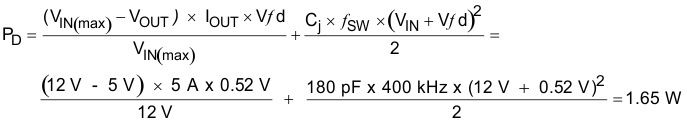
The diode must also be selected with an appropriate power rating. The diode conducts the output current during the off-time of the internal power switch. The off-time of the internal switch is a function of the maximum input voltage, the output voltage, and the switching frequency. The output current during the off-time is multiplied by the forward voltage of the diode to calculate the instantaneous conduction losses of the diode. At higher switching frequencies, the ac losses of the diode need to be taken into account. The ac losses of the diode are due to the charging and discharging of the junction capacitance and reverse recovery charge. Equation 40 is used to calculate the total power dissipation, including conduction losses and ac losses of the diode.
The PDS760 diode has a junction capacitance of 180 pF. Using Equation 40, the total loss in the diode at the nominal input voltage is 1.65 Watts.
If the power supply spends a significant amount of time at light load currents or in sleep mode, consider using a diode which has a low leakage current and slightly higher forward voltage drop.