SLVSBO1G July 2013 – June 2021 TPS54561
PRODUCTION DATA
- 1 Features
- 2 Applications
- 3 Description
- 4 Revision History
- 5 Pin Configuration and Functions
- 6 Specifications
-
7 Detailed Description
- 7.1 Overview
- 7.2 Functional Block Diagram
- 7.3
Feature Description
- 7.3.1 Fixed Frequency PWM Control
- 7.3.2 Slope Compensation Output Current
- 7.3.3 Pulse Skip Eco-mode
- 7.3.4 Low Dropout Operation and Bootstrap Voltage (BOOT)
- 7.3.5 Error Amplifier
- 7.3.6 Adjusting the Output Voltage
- 7.3.7 Enable and Adjusting Undervoltage Lockout
- 7.3.8 Soft Start/Tracking Pin (SS/TR)
- 7.3.9 Sequencing
- 7.3.10 Constant Switching Frequency and Timing Resistor (RT/CLK) Pin)
- 7.3.11 Maximum Switching Frequency
- 7.3.12 Synchronization to RT/CLK Pin
- 7.3.13 Accurate Current Limit Operation
- 7.3.14 Power Good (PWRGD Pin)
- 7.3.15 Overvoltage Protection
- 7.3.16 Thermal Shutdown
- 7.3.17 Small Signal Model for Loop Response
- 7.3.18 Simple Small Signal Model for Peak Current Mode Control
- 7.3.19 Small Signal Model for Frequency Compensation
- 7.4 Device Functional Modes
-
8 Application and Implementation
- 8.1 Application Information
- 8.2
Typical Applications
- 8.2.1
Buck Converter for 7-V to 60-V Input to 5-V at 5-A Output
- 8.2.1.1 Design Requirements
- 8.2.1.2
Detailed Design Procedure
- 8.2.1.2.1 Custom Design with WEBENCH® Tools
- 8.2.1.2.2 Selecting the Switching Frequency
- 8.2.1.2.3 Output Inductor Selection (LO)
- 8.2.1.2.4 Output Capacitor
- 8.2.1.2.5 Catch Diode
- 8.2.1.2.6 Input Capacitor
- 8.2.1.2.7 Slow Start Capacitor
- 8.2.1.2.8 Bootstrap Capacitor Selection
- 8.2.1.2.9 Undervoltage Lockout Set Point
- 8.2.1.2.10 Output Voltage and Feedback Resistors Selection
- 8.2.1.2.11 Compensation
- 8.2.1.2.12 Power Dissipation Estimate
- 8.2.1.2.13 Safe Operating Area
- 8.2.1.2.14 Discontinuous Conduction Mode and Eco-mode Boundary
- 8.2.1.3 Application Curves
- 8.2.2 Inverting Buck-Boost Topology for Positive Input to Negative Output
- 8.2.3 Split-Rail Topology for Positive Input to Negative and Positive Output
- 8.2.1
Buck Converter for 7-V to 60-V Input to 5-V at 5-A Output
- 9 Power Supply Recommendations
- 10Layout
- 11Device and Documentation Support
- 12Mechanical, Packaging, and Orderable Information
Package Options
Mechanical Data (Package|Pins)
- DPR|10
Thermal pad, mechanical data (Package|Pins)
Orderable Information
8.2.1.2.11 Compensation
There are several methods to design compensation for DC-DC regulators. The method presented here is easy to calculate and ignores the effects of the slope compensation that is internal to the device. Since the slope compensation is ignored, the actual crossover frequency will be lower than the crossover frequency used in the calculations. This method assumes the crossover frequency is between the modulator pole and the ESR zero and the ESR zero is at least 10 times greater the modulator pole.
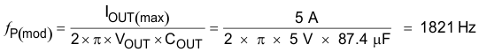
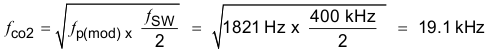
To get started, the modulator pole, ƒp(mod), and the ESR zero, ƒz1 must be calculated using Equation 48 and Equation 49. For COUT, use a derated value of 87.4 μF. Use equations Equation 50 and Equation 51 to estimate a starting point for the crossover frequency, ƒco. For the example design, ƒp(mod) is 1821 Hz and ƒz(mod) is 1100 kHz. Equation 49 is the geometric mean of the modulator pole and the ESR zero and Equation 51 is the mean of modulator pole and half of the switching frequency. Equation 50 yields 44.6 kHz and Equation 51 gives 19.1 kHz. Use the geometric mean value of Equation 50 and Equation 51 for an initial crossover frequency. For this example, after lab measurement, the crossover frequency target was increased to 30 kHz for an improved transient response.
Next, the compensation components are calculated. A resistor in series with a capacitor is used to create a compensating zero. A capacitor in parallel to these two components forms the compensating pole.


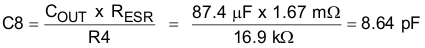
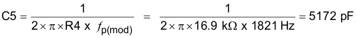
To determine the compensation resistor, R4, use Equation 52. Assume the power stage transconductance, gmps, is 17 A/V. The output voltage, VO, reference voltage, VREF, and amplifier transconductance, gmea, are 5 V, 0.8 V, and 350 μA/V, respectively. R4 is calculated to be 16.8 kΩ and a standard value of 16.9 kΩ is selected. Use Equation 53 to set the compensation zero to the modulator pole frequency. Equation 53 yields 5172 pF for compensating capacitor C5. 4700 pF is used for this design.

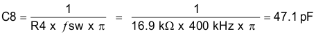
A compensation pole can be implemented if desired by adding capacitor C8 in parallel with the series combination of R4 and C5. Use the larger value calculated from Equation 54 and Equation 55 for C8 to set the compensation pole. The selected value of C8 is 47 pF for this design example.