SLVSDC9B November 2016 – November 2019 TPS54824
PRODUCTION DATA.
- 1 Features
- 2 Applications
- 3 Description
- 4 Revision History
- 5 Pin Configuration and Functions
- 6 Specifications
-
7 Detailed Description
- 7.1 Overview
- 7.2 Functional Block Diagram
- 7.3
Feature Description
- 7.3.1 Fixed Frequency PWM Control
- 7.3.2 Continuous Conduction Mode Operation (CCM)
- 7.3.3 VIN Pins and VIN UVLO
- 7.3.4 Voltage Reference and Adjusting the Output Voltage
- 7.3.5 Error Amplifier
- 7.3.6 Enable and Adjustable UVLO
- 7.3.7 Soft Start and Tracking
- 7.3.8 Safe Start-up into Pre-Biased Outputs
- 7.3.9 Power Good
- 7.3.10 Sequencing (SS/TRK)
- 7.3.11 Adjustable Switching Frequency (RT Mode)
- 7.3.12 Synchronization (CLK Mode)
- 7.3.13 Bootstrap Voltage and 100% Duty Cycle Operation (BOOT)
- 7.3.14 Output Overvoltage Protection (OVP)
- 7.3.15 Overcurrent Protection
- 7.4 Device Functional Modes
-
8 Application and Implementation
- 8.1 Application Information
- 8.2
Typical Application
- 8.2.1 Design Requirements
- 8.2.2
Detailed Design Procedure
- 8.2.2.1 Switching Frequency
- 8.2.2.2 Output Inductor Selection
- 8.2.2.3 Output Capacitor
- 8.2.2.4 Input Capacitor
- 8.2.2.5 Output Voltage Resistors Selection
- 8.2.2.6 Soft-start Capacitor Selection
- 8.2.2.7 Undervoltage Lockout Set Point
- 8.2.2.8 Bootstrap Capacitor Selection
- 8.2.2.9 PGOOD Pull-up Resistor
- 8.2.2.10 Compensation
- 8.2.3 Application Curves
- 9 Power Supply Recommendations
- 10Layout
- 11Device and Documentation Support
- 12Mechanical, Packaging, and Orderable Information
Package Options
Mechanical Data (Package|Pins)
- RNV|18
Thermal pad, mechanical data (Package|Pins)
Orderable Information
7.3.12 Synchronization (CLK Mode)
An internal Phase Locked Loop (PLL) has been implemented to allow synchronization from 200 kHz to 1600 kHz, and to easily switch from RT mode to CLK mode. To implement the synchronization feature, connect a square wave clock signal to the RT/CLK pin with a duty cycle from 20% to 80%. If the clock signals rising edge occurs near the falling edge of SW, increased SW jitter may occur. Use Equation 11 to calculate the maximum clock pulse width to minimize jitter in CLK mode. The clock signal amplitude must transition lower than 0.8 V and higher than 2 V. The start of the switching cycle is synchronized to the falling edge of the RT/CLK pin.

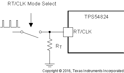
In applications where both RT mode and CLK mode are needed, the device can be configured as shown in Figure 28. Before the external clock is present, the device works in RT mode and the switching frequency is set by RT resistor. When the external clock is present, the CLK mode overrides the RT mode. The first time the SYNC pin is pulled above the RT/CLK high threshold (2 V), the device switches from the RT mode to the CLK mode and the RT/CLK pin becomes high impedance as the PLL starts to lock onto the frequency of the external clock.
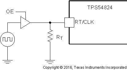
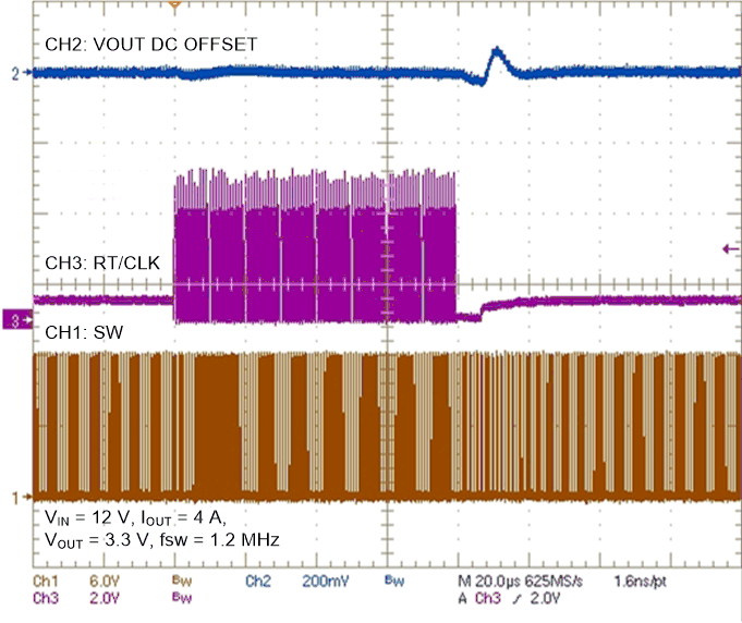
If the input clock goes away the internal clock frequency begins to drop and after 10 µs without a clock the device returns to RT mode. Output undershoot while the switching frequency drops can occur. Output overshoot can also occur when the switching frequency steps back up to the RT mode frequency. A high impedance tri-state buffer as shown in Figure 30 is recommended for best performance during the transition from CLK mode to RT mode because it minimizes the loading on the RT/CLK pin allowing faster transition back to RT mode. Figure 31 shows the typical performance for the transition from RT mode to CLK mode then back to RT mode.
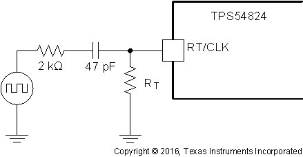
A series RC circuit as shown in Figure 29 can also be used to interface the RT/CLK pin but the capacitive load slows down the transition back to RT mode. The series RC circuit is not recommended if the transition from CLK mode to RT mode is important. A capacitor in the range of 47 pF to 470 pF is recommended. When using the series RC circuit verify the amplitude of the signal at the RT/CLK pin goes above the high threshold.
 Figure 28. Simplified Circuit When Using Both RT Mode and CLK Mode
  Figure 29. Interfacing to the RT/CLK Pin with Series RC
  Figure 30. Interfacing to the RT/CLK Pin with Buffer
  Figure 31. RT to CLK to RT Transition with Buffer