SLUSC70D March   2016  – July 2017 TPS548D22

PRODUCTION DATA.  

  1. Features
  2. Applications
  3. Description
    1.     Device Images
      1.      Simplified Application
  4. Revision History
  5. Pin Configuration and Functions
    1.     Pin Functions
  6. Specifications
    1. 6.1 Absolute Maximum Ratings
    2. 6.2 ESD Ratings
    3. 6.3 Recommended Operating Conditions
    4. 6.4 Thermal Information
    5. 6.5 Electrical Characteristics
    6. 6.6 Typical Characteristics
  7. Detailed Description
    1. 7.1 Overview
    2. 7.2 Functional Block Diagram
    3. 7.3 Feature Description
      1. 7.3.1 40-A FET
      2. 7.3.2 On-Resistance
      3. 7.3.3 Package Size, Efficiency and Thermal Performance
      4. 7.3.4 Soft-Start Operation
      5. 7.3.5 VDD Supply Undervoltage Lockout (UVLO) Protection
      6. 7.3.6 EN_UVLO Pin Functionality
      7. 7.3.7 Fault Protections
        1. 7.3.7.1 Current Limit (ILIM) Functionality
        2. 7.3.7.2 VDD Undervoltage Lockout (UVLO)
        3. 7.3.7.3 Overvoltage Protection (OVP) and Undervoltage Protection (UVP)
        4. 7.3.7.4 Out-of-Bounds Operation
        5. 7.3.7.5 Overtemperature Protection
    4. 7.4 Device Functional Modes
      1. 7.4.1 DCAP3 Control Topology
      2. 7.4.2 DCAP Control Topology
    5. 7.5 Programming
      1. 7.5.1 Programmable Pin-Strap Settings
        1. 7.5.1.1 Frequency Selection (FSEL) Pin
        2. 7.5.1.2 VSEL Pin
        3. 7.5.1.3 DCAP3 Control and Mode Selection
          1. 7.5.1.3.1 Application Workaround to Support 4-ms and 8-ms SS Settings
      2. 7.5.2 Programmable Analog Configurations
        1. 7.5.2.1 RSP/RSN Remote Sensing Functionality
          1. 7.5.2.1.1 Output Differential Remote Sensing Amplifier
        2. 7.5.2.2 Power Good (PGOOD Pin) Functionality
  8. Application and Implementation
    1. 8.1 Application Information
    2. 8.2 Typical Applications
      1. 8.2.1 TPS548D22 1.5-V to 16-V Input, 1-V Output, 40-A Converter
      2. 8.2.2 Design Requirements
      3. 8.2.3 Design Procedure
        1. 8.2.3.1  Switching Frequency Selection
        2. 8.2.3.2  Inductor Selection
        3. 8.2.3.3  Output Capacitor Selection
          1. 8.2.3.3.1 Minimum Output Capacitance to Ensure Stability
          2. 8.2.3.3.2 Response to a Load Transient
          3. 8.2.3.3.3 Output Voltage Ripple
        4. 8.2.3.4  Input Capacitor Selection
        5. 8.2.3.5  Bootstrap Capacitor Selection
        6. 8.2.3.6  BP Pin
        7. 8.2.3.7  R-C Snubber and VIN Pin High-Frequency Bypass
        8. 8.2.3.8  Optimize Reference Voltage (VSEL)
        9. 8.2.3.9  MODE Pin Selection
        10. 8.2.3.10 Overcurrent Limit Design.
      4. 8.2.4 Application Curves
  9. Power Supply Recommendations
  10. 10Layout
    1. 10.1 Layout Guidelines
    2. 10.2 Layout Example
      1. 10.2.1 Mounting and Thermal Profile Recommendation
  11. 11Device and Documentation Support
    1. 11.1 Device Support
      1. 11.1.1 Third-Party Products Disclaimer
    2. 11.2 Receiving Notification of Documentation Updates
    3. 11.3 Community Resources
    4. 11.4 Trademarks
    5. 11.5 Electrostatic Discharge Caution
    6. 11.6 Glossary
  12. 12Mechanical, Packaging, and Orderable Information

Package Options

Mechanical Data (Package|Pins)
Thermal pad, mechanical data (Package|Pins)
Orderable Information

Typical Characteristics

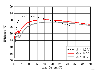
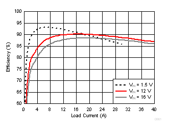
TPS548D22 D011_SLUSC70.gif
VOUT = 1 V SKIP Mode fSW = 650 kHz
VDD = 5 V
Figure 1. Efficiency vs Output Current
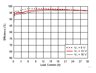
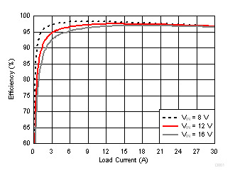
TPS548D22 D013_slusc70.gif
VOUT = 5.5 V SKIP Mode fSW = 425 kHz
VDD = 5 V
Figure 3. Efficiency vs Output Current
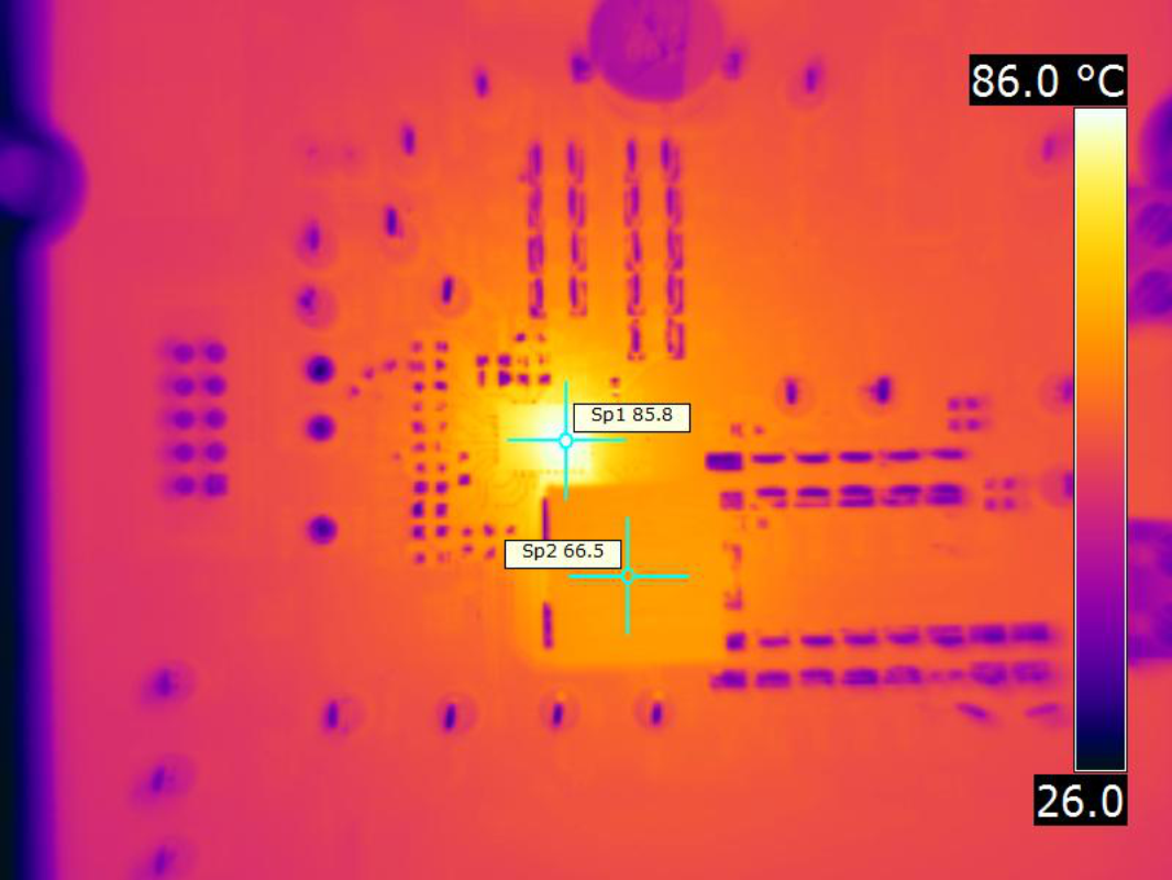
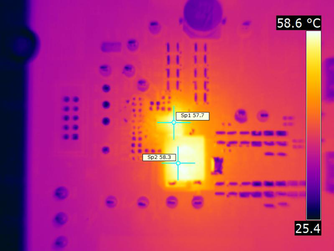
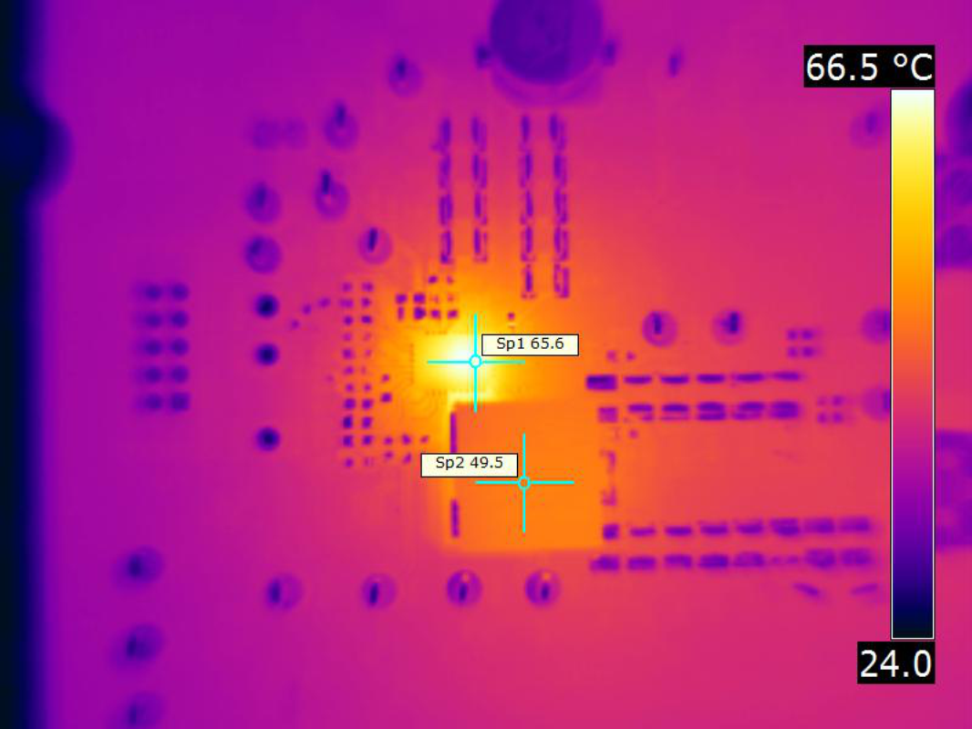
TPS548D22 figure5_thermal_slusc70.png
VIN = 12 V fSW = 650 kHz IOUT = 40 A
VOUT = 1 V Natural convection
Figure 5. Thermal Image
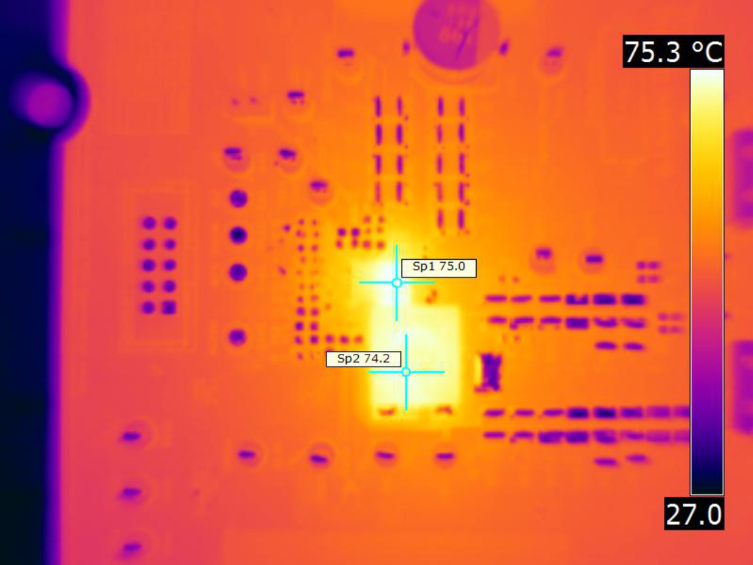
TPS548D22 figure7_thermal_slusc70.png
VIN = 12 V fSW = 650 kHz IOUT = 40 A
VOUT = 1 V Airflow = 400 LFM
Figure 7. Thermal Image
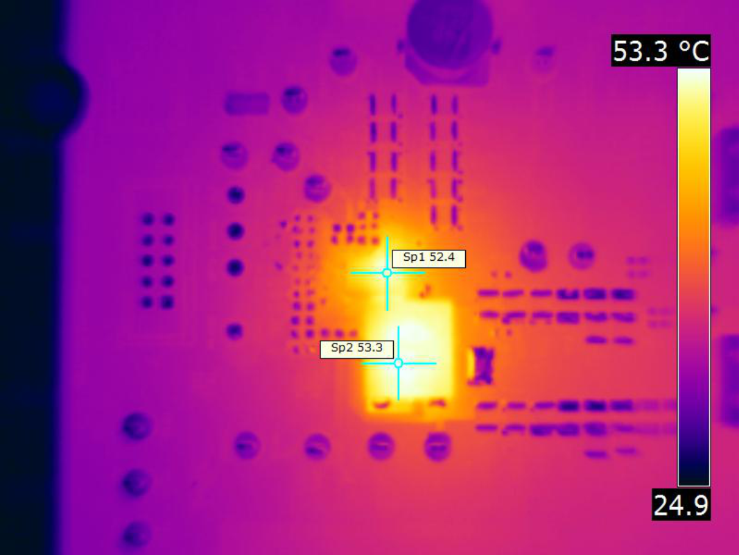
TPS548D22 figure9_thermal_slusc70.png
VIN = 12 V fSW = 425 kHz IOUT = 30 A
VOUT = 5.5 V Airflow = 200 LFM
Figure 9. Thermal Image
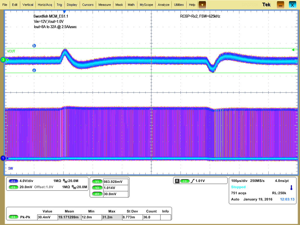
TPS548D22 wave_7_p2p_2.png
VOUT = 1 V VIN = 12 V
IOUT from 8 A to 32 A 2.5 A/µs
Figure 11. Transient Response Peak-to-Peak
TPS548D22 D012_SLUSC70.gif
VOUT = 1 V FCCM fSW = 650 kHz
VDD = 5 V
Figure 2. Efficiency vs Output Current
TPS548D22 D014_slusc70.gif
VOUT = 5.5 V FCCM fSW = 425 kHz
VDD = 5 V
Figure 4. Efficiency vs Output Current
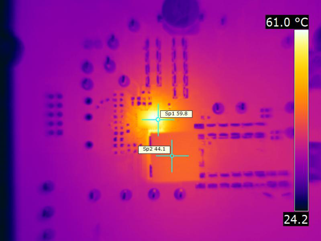
TPS548D22 figure6_thermal_slusc70.png
VIN = 12 V fSW = 650 kHz IOUT = 40 A
VOUT = 1 V Airflow = 200 LFM
Figure 6. Thermal Image
TPS548D22 figure8_thermal_slusc70.png
VIN = 12 V fSW = 425 kHz IOUT = 30 A
VOUT = 5.5 V Natural convection
Figure 8. Thermal Image
TPS548D22 figure10_thermal_slusc70.png
VIN = 12 V fSW = 425 kHz IOUT = 30 A
VOUT = 5.5 V Airflow = 400 LFM
Figure 10. Thermal Image