SLVS939B June 2009 – December 2014 TPS55332-Q1
PRODUCTION DATA.
- 1 Features
- 2 Applications
- 3 Description
- 4 Revision History
- 5 Pin Configuration and Functions
- 6 Specifications
-
7 Detailed Description
- 7.1 Overview
- 7.2 Functional Block Diagram
- 7.3
Feature Description
- 7.3.1 Input Voltage (VIN)
- 7.3.2 Output Voltage (Vout)
- 7.3.3 Regulated Supply Voltage (VReg)
- 7.3.4 Over-Current Protection (SW)
- 7.3.5 Oscillator Frequency (RT)
- 7.3.6 Enable / Shutdown (EN)
- 7.3.7 Reset Delay (Cdly)
- 7.3.8 Reset Pin (RST)
- 7.3.9 Boost Capacitor (BOOT)
- 7.3.10 Soft Start (SS)
- 7.3.11 Synchronization (SYNC)
- 7.3.12 Regulation Voltage (VSENSE)
- 7.3.13 Reset Threshold (RST_TH)
- 7.3.14 Slew Rate Control (Rslew)
- 7.3.15 Thermal Shutdown
- 7.3.16 Loop Control Frequency Compensation
- 7.4 Device Functional Modes
-
8 Application and Implementation
- 8.1 Application Information
- 8.2
Typical Application
- 8.2.1 Design Requirements
- 8.2.2
Detailed Design Procedure
- 8.2.2.1 Output Capacitor (Co)
- 8.2.2.2 Output Inductor Selection (Lo) for CCM
- 8.2.2.3 Output Diode
- 8.2.2.4 Input Capacitor CI
- 8.2.2.5 Output Voltage And Feedback Resistor Selection
- 8.2.2.6 Reset Threshold Resistor Selection
- 8.2.2.7 Soft Start Capacitor
- 8.2.2.8 Loop Compensation Calculation
- 8.2.2.9 Loop Compensation Response
- 8.2.2.10 Output Inductor Selection (LO) For DCM
- 8.2.3 Application Curves
- 9 Power Supply Recommendations
- 10Layout
- 11Device and Documentation Support
- 12Mechanical, Packaging, and Orderable Information
Package Options
Mechanical Data (Package|Pins)
- PWP|20
Thermal pad, mechanical data (Package|Pins)
- PWP|20
Orderable Information
8 Application and Implementation
NOTE
Information in the following applications sections is not part of the TI component specification, and TI does not warrant its accuracy or completeness. TI’s customers are responsible for determining suitability of components for their purposes. Customers should validate and test their design implementation to confirm system functionality.
8.1 Application Information
The TPS55332-Q1 device can function as a switch mode boost converter along with voltage supervisor. The system can function at input voltage as low as 1.5 V once the internal circuits have stabilized. The supervisor circuit monitors the regulated output and indicates when the output voltage has fallen below the set value. The variable switching frequency allows use of low profile inductors and low value input and output capacitors.
8.2 Typical Application
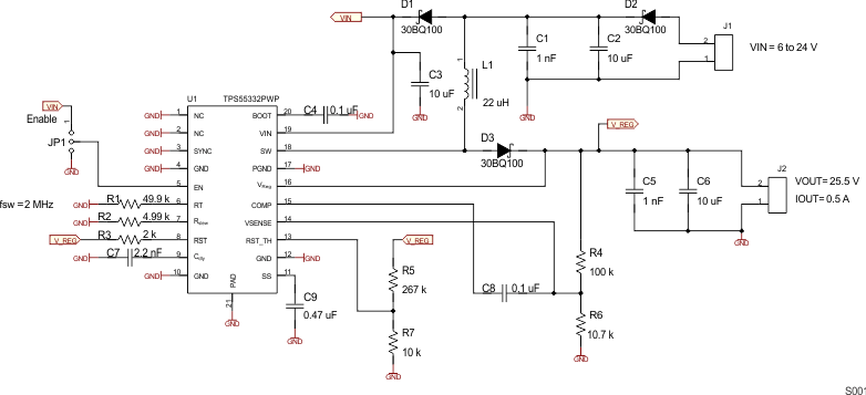 Figure 11. Typical Application Schematic
8.2.1 Design Requirements
Table 1 table lists the requirements of a switching regulator design.
Table 1. Design Parameters
| PARAMETER | VALUE |
|---|---|
| Input voltage, VIN | 6 V to 24 V, with typical operating voltage = 14 V |
| Output voltage, V | 25.5 V ± 2% |
| Maximum output current, IO | 0.5 A |
| Transient response 0A to 0.3 A | 5% |
| Switching frequency, ƒsw | 2 MHz |
| Reset threshold | 84% of output voltage |
| Vo_ripple | 520 mV peak to peak at capacitance |
| Vo_transient | 92% of output voltage |
8.2.2 Detailed Design Procedure
The design considers the converter to operate in CCM for most of the operating range and in DCM during less than 10% of the maximum load rating. CCM mode has an RHP of zero. Thus, compensation becomes critical under CCM mode. Operating the converter in DCM mode results in higher switch and inductor currents and thereby higher losses. In this design example, we focus on circuit operating mostly under CCM mode.
8.2.2.1 Output Capacitor (Co)
Selection of the output capacitor in CCM using Equation 19 gives a capacitor value of 0.37 μF.
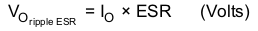
Output ripple voltage is a product of output capacitor ESR and ripple current on the output capacitor Co.
The minimum output capacitor required for a desired output ripple voltage is given by:
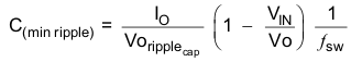
The minimum capacitance needed for the output voltage ripple specification, using Equation 19, C ↓(min ↓ ripple) = 0.37 μF.
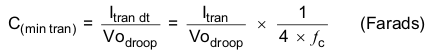
Using Equation 20, the transient response should be taken into consideration when selecting the output capacitor. The minimum capacitance required for a duration dt with a load transient Itran to allow a maximum output voltage droop of Vo_droop is:
Where,
dt is approximated to 1 / 4 × ƒc ( ƒc = 10 kHz bandwidth)
This gives a capacitance of 7.35 μF. Allowing for tolerances and temperature variations, use a 10 μF standard value output capacitor.
8.2.2.2 Output Inductor Selection (Lo) for CCM
Using Equation 21, the minimum lead current for ccm operation is 10% of maximum output current, IO-DCM = 50 mA. The inductor value is selected as L = 22 μH.
8.2.2.3 Output Diode
The TPS55332 requires an external output diode which conducts when the power switch is turned off. This provides the path for the inductor current to the output capacitor. The important factors in selecting the rectifier are: fast switching, reverse breakdown voltage, current rating, and forward-voltage drop. The breakdown voltage should be greater than the maximum output voltage; the current rating must be two times the maximum switch output current. The forward drop of the diode should be low (schottky rectifier is preferred). The schottky diode is selected based on the appropriate power rating, which factors in the dc conduction losses; this is determined by Equation 27:

Where,
Vƒd = forward conducting voltage of Schottky diode
8.2.2.4 Input Capacitor CI
The TPS55332 requires an input ceramic de-coupling capacitor type X5R or X7R and bulk capacitance to minimize input ripple voltage. The dc voltage rating of this input capacitance must be greater than the maximum input voltage. The capacitor must have an input ripple current rating higher than the maximum input ripple current of the converter for the application; this is determined by Equation 28.
The input capacitors for power regulators are chosen to have a reasonable capacitance to volume ratio and be fairly stable over the temperature range.
8.2.2.5 Output Voltage And Feedback Resistor Selection
In the design example, 100 kΩ was selected for R4, using Equation 1, R6 is calculated as 10.7 kΩ. Higher resistor values help improve converter efficiency at low output currents but may introduce noise immunity problems.
8.2.2.6 Reset Threshold Resistor Selection
Using Equation 6, select resistor R7 as 10 kΩ then calculate R5. This gives a resistor value of 263 kΩ; use a standard value of 267 kΩ. This sets the reset threshold at 0.86 × 25.5 V.
8.2.2.7 Soft Start Capacitor
The soft start capacitor determines the minimum time to reach the desired output voltage during a power up cycle. This is useful when a load requires a controlled voltage slew rate and helps to limit the current draw from the input voltage supply line. Equation 4 and Equation 5 have to be satisfied in addition to the other conditions stated in the soft start section of this document. In this design a 47-nF capacitor is required to meet these criteria.
8.2.2.8 Loop Compensation Calculation
To make sure the right hand plane zero does not impact converter design in CCM operation based on VIN = 6 V, L = 22 μH, and Co = 10 μf, calculated values using Equation 16, the frequency is set at:
ƒRHP = 20.436 kHz
The double pole associated with the L and Co components is given by Equation 15:
ƒLC = 2.526 kHz
Using Equation 14:
ƒC = 6.744 kHz
The zero due to the ESR of the capacitor is beyond the right hand plane zero frequency and can be calculated based on Equation 17 and Equation 23.
So to avoid any instability issues and from the frequency values calculated above the amplifier gain requires a gain roll off much earlier than the double pole of the L and Co components.
So the pole must be set at a much lower frequency to obtain a reasonable phase margin.
Using Equation 18 and choosing a frequency close to 2.9 Hz for the pole frequency, the capacitor value C8 for this application is:
C8 = 0.54 μF
If C8 = 0.1 μF standard value, then ƒP = 15.9 Hz.
8.2.2.9 Loop Compensation Response
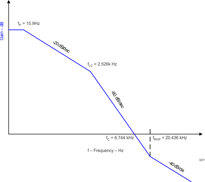 Figure 12. Loop Compensation Response
Since the pole due to the integrating capacitor C4 is dominant in the compensation loop, the frequency of the pole due to the inductor has no consequence in this situation.
8.2.2.10 Output Inductor Selection (LO) For DCM
The maximum inductor value is calculated using Equation 16 and gives a value of 0.532 μH. This allows the converter to be in DCM mode over the full operating range.
To operate in this mode with the calculated inductor value, the right hand plane zero frequency has moved to 846 kHz and the cut off frequency is 279.1 kHz.
The double pole due to the L and Co values is 16.25 kHz.
To compensate with either type II or type III loop compensation, the Bode Plot stability criteria must be satisfied.
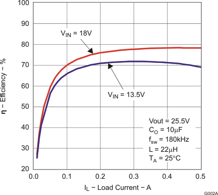
Figure 14 shows the Efficiency readings for TPS55332 running mostly in DCM mode. When the switching frequency is reduced from 2 MHz to 180 kHz, keeping the Inductance and output load fixed, the converter sees higher peak currents in the switch and inductor. Higher currents lead to losses and thus efficiency readings come out to be lower than when the converter runs in CCM mode.
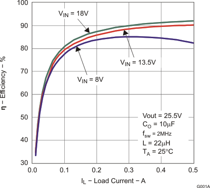
8.2.3 Application Curves