SLVS939B June 2009 – December 2014 TPS55332-Q1
PRODUCTION DATA.
- 1 Features
- 2 Applications
- 3 Description
- 4 Revision History
- 5 Pin Configuration and Functions
- 6 Specifications
-
7 Detailed Description
- 7.1 Overview
- 7.2 Functional Block Diagram
- 7.3
Feature Description
- 7.3.1 Input Voltage (VIN)
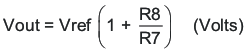
- 7.3.2 Output Voltage (Vout)
- 7.3.3 Regulated Supply Voltage (VReg)
- 7.3.4 Over-Current Protection (SW)
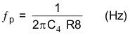
- 7.3.5 Oscillator Frequency (RT)
- 7.3.6 Enable / Shutdown (EN)
- 7.3.7 Reset Delay (Cdly)
- 7.3.8 Reset Pin (RST)
- 7.3.9 Boost Capacitor (BOOT)
- 7.3.10 Soft Start (SS)
- 7.3.11 Synchronization (SYNC)
- 7.3.12 Regulation Voltage (VSENSE)
- 7.3.13 Reset Threshold (RST_TH)
- 7.3.14 Slew Rate Control (Rslew)
- 7.3.15 Thermal Shutdown
- 7.3.16 Loop Control Frequency Compensation
- 7.4 Device Functional Modes
-
8 Application and Implementation
- 8.1 Application Information
- 8.2
Typical Application
- 8.2.1 Design Requirements
- 8.2.2
Detailed Design Procedure
- 8.2.2.1 Output Capacitor (Co)
- 8.2.2.2 Output Inductor Selection (Lo) for CCM
- 8.2.2.3 Output Diode
- 8.2.2.4 Input Capacitor CI
- 8.2.2.5 Output Voltage And Feedback Resistor Selection
- 8.2.2.6 Reset Threshold Resistor Selection
- 8.2.2.7 Soft Start Capacitor
- 8.2.2.8 Loop Compensation Calculation
- 8.2.2.9 Loop Compensation Response
- 8.2.2.10 Output Inductor Selection (LO) For DCM
- 8.2.3 Application Curves
- 9 Power Supply Recommendations
- 10Layout
- 11Device and Documentation Support
- 12Mechanical, Packaging, and Orderable Information
Package Options
Mechanical Data (Package|Pins)
- PWP|20
Thermal pad, mechanical data (Package|Pins)
- PWP|20
Orderable Information
7 Detailed Description
7.1 Overview
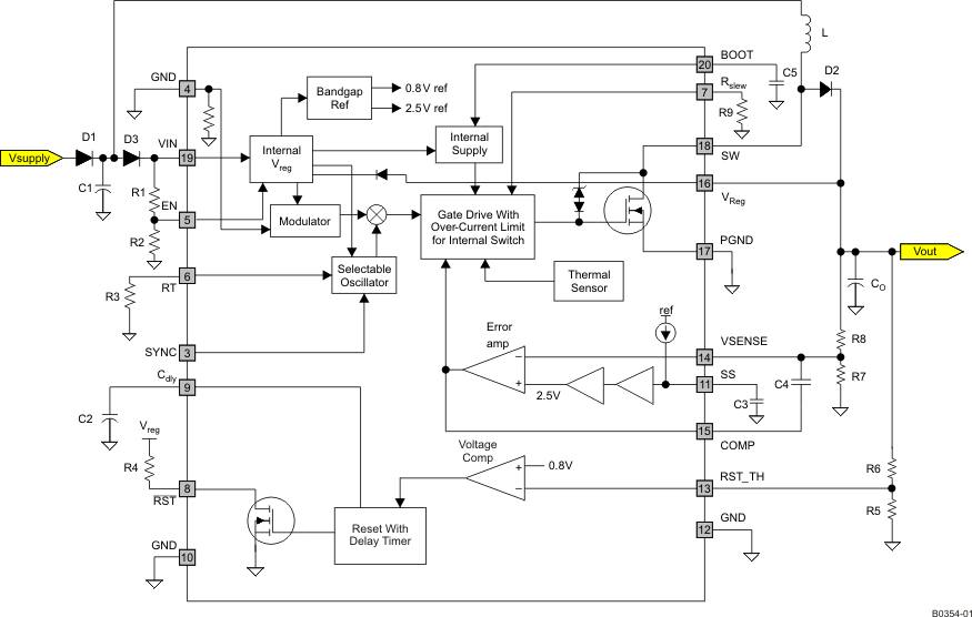
The TPS55332 operates as a step up (boost) converter; the feedback concept is voltage mode control using the VSENSE terminal, with cycle-by-cycle current limit.
The voltage supervisory function for power-on-rest during system power-on is monitoring the output voltage, and once this has exceeded the threshold set by RST_TH, a delay of 1.0 ms/nF (based on the capacitor value on the Cdly terminal) is invoked before the RST line is released high. Conversely, on power down, once the output voltage falls below the same set threshold (ignoring hysteresis), RST is pulled low only after a de-glitch filter of approximately 20 μs (typ) expires. This is implemented to prevent RST from being triggered due to fast transient noise on the output supply.
Soft start is activated on every enable cycle and limits the power stored in the inductor by duty cycle control. Soft start duration is set by an external capacitor on the SS terminal.
If thermal shutdown is invoked due to excessive power dissipation, the internal switch is disabled and the regulated output voltage starts to decrease. Depending on the load line, the regulated voltage can decay and the RST_TH threshold may assert RST output low after the output voltage drops below the set threshold.
7.2 Functional Block Diagram
7.3 Feature Description
The TPS55332 is a step up (boost) dc/dc converter using voltage-control mode scheme. The following sections include descriptions of the individual pin functions.
7.3.1 Input Voltage (VIN)
The VIN pin is the input power source for the TPS55332. This pin must be externally protected against voltage level transients greater than 60 V and reverse battery. In boost mode the input current drawn from this pin is pulsed, with fast rise and fall times. Therefore, this input line requires a filter capacitor to minimize noise. Additionally, for EMI considerations, an input filter inductor may also be required.
7.3.2 Output Voltage (Vout)
The output voltage, Vout, is generated by the converter supplied from the battery voltage VIN and external components (L, C). The output is sensed through an external resistor divider and compared with an internal reference voltage.
The value of the adjustable output voltage in boost mode is selectable between VIN × 1.05 to 50 V if the minimum ON time (ton) and minimum OFF times are NOT violated by choosing the external resistors, according to the following relationship:
Where:
R7 and R8 are feedback resistors
Vref = 2.5 V (typ)
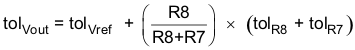
The internal reference voltage Vref has a ±1.5% tolerance. The overall output voltage tolerance is dependent on the external feedback resistors. To determine the overall output voltage tolerance, use the following relationship:
Typically, an output capacitor within the range of 10 μF to 400 μF is used. This terminal has a filter capacitor with low ESR characteristics in order to minimize output ripple voltage.
7.3.3 Regulated Supply Voltage (VReg)
There is an integrated forward biased diode between VReg and VIN. VReg is tied to Vout and used to bias VIN when Vout > Vsupply.
7.3.4 Over-Current Protection (SW)
Over-current protection is implemented by sensing the current through the NMOS switch FET. The sensed current is then compared to a current reference level representing the over-current threshold limit. If the sensed current exceeds the over-current threshold limit, the over-current indicator is set true. The system ignores the over-current indicator for the leading edge blanking time at the beginning of each cycle to avoid any turn-on noise glitches.
Once the over-current indicator is set true, over-current protection is triggered. The MOSFET is turned off for the rest of the cycle after a propagation delay. The over-current protection scheme is called cycle-by-cycle current limiting. If the sensed current continues to increase during cycle-by-cycle current limiting, the temperature of the device starts to rise, and the TSD kicks in and shuts down switching until the device cools down.
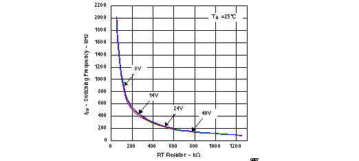
7.3.5 Oscillator Frequency (RT)
The oscillator frequency is selectable by means of a resistor placed at the RT pin. The switching frequency (ƒsw) can be set in the range of 80 kHz to 2.2 MHz. In addition, the switching frequency can be imposed externally by a clock signal (ƒext) at the SYNC pin with ƒsw < ƒext < 2 × ƒsw. In this case the external clock overrides the switching frequency determined by the RT pin, and the internal oscillator is clocked by the external synchronization clock input.
7.3.6 Enable / Shutdown (EN)
The Enable pin provides electrical on/off control of the regulator. Once the Enable pin voltage exceeds the threshold voltage, the regulator starts operation and the internal soft start begins to ramp. If the Enable pin voltage is pulled below the threshold voltage, the regulator stops switching and the internal soft start resets. Connecting the pin to ground or to any voltage less than 0.7 V disables the regulator and activates shutdown mode. The quiescent current of the TPS55332 in shutdown mode is typically < 2 μA. This pin has to have an external pull up or pull down to change the state of the device.
7.3.7 Reset Delay (Cdly)
The Reset delay pin sets the desired delay time for asserting the RST pin high after the supply has exceeded the programmed Vreg_RST voltage. The delay may be programmed in the range of 2.2 ms to 200 ms using capacitors in the range of 2.2 nF to 200 nF. The delay time is calculated using Equation 3:

7.3.8 Reset Pin (RST)
The RST pin is an open-drain output. The power-on reset output is asserted low until the output voltage exceeds the programmed Vreg_RST voltage threshold and the reset delay timer has expired. Additionally, whenever the Enable pin is low or open, RST is immediately asserted low regardless of the output voltage. There is a reset de-glitch timer to prevent a reset being invoked due to short negative transients on the output line. If a thermal shut down occurs due to excessive thermal conditions this pin is asserted low, where switching is commanded off and the output drops below the rest threshold set on the RST_TH terminal.
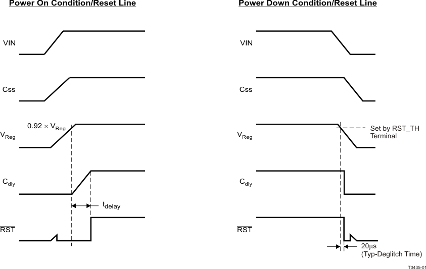 Figure 6. Reset Line Conditions
7.3.9 Boost Capacitor (BOOT)
This capacitor provides gate drive voltage for the Internal MOSFET switch. X7R or X5R grade dielectrics are recommended due to their stable values over temperature.
7.3.10 Soft Start (SS)
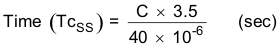
To limit the start-up inrush current, an internal soft start circuit is used to ramp up the reference voltage from 0 V to its final value. The switch duty cycle starts with narrow pulses and increases gradually as the voltage on the Css capacitor ramps up. The output current on this pin charges the capacitor up to 6.6 V (typ).
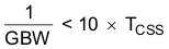
The boost soft start is dependent on the gain bandwidth (GBW) of the loop. Therefore, in this configuration the Css equation only holds when:
GBW is dependent on the compensation technique used. TYPE1 is the slowest.
Where:
Tcss is the time it takes for Vcss to reach ~3.5 V
GBW = ƒc of the converter
Where:
C = Capacitor Css on the SS pin
7.3.11 Synchronization (SYNC)
The SYNC pin inputs an external clock signal that synchronizes the switching frequency. The synchronization input over-rides the internally fixed oscillator signal. The synchronization signal has to be valid for approximately 2 clock cycles (pulses) before the transition is made for synchronization with the external frequency input. If the external clock input is does NOT transition low or high for 32 μs (typ), the system defaults to the internal clock set by the Rosc pin.
7.3.12 Regulation Voltage (VSENSE)
This pin is used to program the regulated output voltage based on a resistor feedback network monitoring the Vout voltage. The selected ratio of R7 and R8 sets the output voltage.
7.3.13 Reset Threshold (RST_TH)
This pin is programmable to set the under-voltage monitoring of the regulated output voltage. The resistor combination of R5 and R6 is used to program the threshold for detection of under-voltage.
Recommended range: 70% to 92% of the regulation voltage
The internal reference Vref is set at 0.8 V ±1.5%
7.3.14 Slew Rate Control (Rslew)
This pin controls the switching slew rate of the internal power NMOS. The slew rate is set by an external resistor with a slew rate range shown for rise and fall times. The range of rise time tr = 20 ns to 60 ns and fall time tf = 60 ns to 250 ns, with Rslew range of 5 kΩ to 20 kΩ (see Figure 7 and Figure 8).
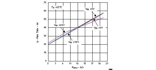 Figure 7. Fet Rise Time (Tr)
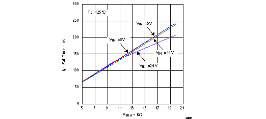 Figure 8. Fet Fall Time (Tf)
7.3.15 Thermal Shutdown
The TPS55332 device protects itself from overheating with an internal thermal shutdown circuit. If the junction temperature exceeds the thermal shutdown trip point, the MOSFET is turned off. The device is restarted under control of the slow start circuit automatically when the junction temperature drops below the thermal shutdown hysteresis trip point.
7.3.16 Loop Control Frequency Compensation
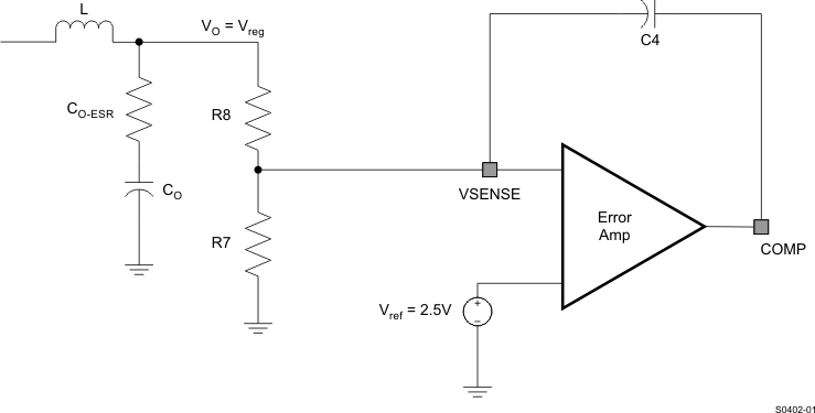 Figure 9. Type 1 Compensation
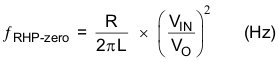
The boost converter operating in continuous conduction mode (CCM) has a right-half-plane (RHP) zero with the transfer function. The RHP zero causes the converter to respond to a circuit disturbance in the opposite direction to that needed to support the output load transition (positive feedback). This complicates loop compensation and limits the converter bandwidth, and requires an increase in the output filter capacitor.
The converter can be designed to operate in discontinuous conduction mode (DCM) with a smaller inductance value for the inductor over the full range of the operating conditions. This may be difficult to achieve and other issues like instability may occur if the converter enters CCM.
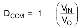
The inductor saturation current Isat must satisfy the following:
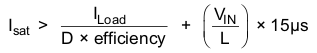
Where:
D = VIN/VO
The converter designed for CCM with external loop compensation factors the maximum output load current, the ESR of the output filter capacitor, the inductance used for the inductor, the input voltage range, and the output voltage required.
7.4 Device Functional Modes
7.4.1 DCM Operation
The control to output transfer function for the boost in DCM has a single pole. The energy in the inductor is completely discharged during every switching cycle (inductor current is reduced to zero). The small inductor value for DCM compared to CCM operation shifts the RHP zero frequency close to the switching frequency, see Equation 11. In this mode, the RHP is not a factor for compensation of the feedback loop, additionally the frequency of the pole associated with the inductor is also increased to a higher frequency.
The maximum inductance to keep the boost converter running in DCM over the full operating range is given by Equation 8:
Where:
VO = Output voltage
IO = Maximum output current
VIN = Minimum input voltage
Three elements of the output capacitor contribute to the impedance (output voltage ripple), ESR, ESL, and capacitance.
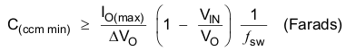
During discontinuous conduction mode operation, the minimum capacitance needed to limit the voltage ripple due to the capacitance of the capacitor is given by Equation 10:
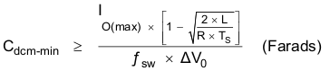
Where:
R = min load resistance,
Ts = clock period,
ƒsw = switching frequency,
ΔV0 = output voltage ripple desired
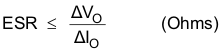
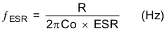
The ESR of the output capacitor needed to limit the output ripple voltage is given by Equation 11:
7.4.2 CCM Operation
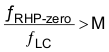
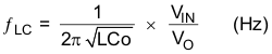
In continuous conduction mode of operation the RHP zero complicates the loop compensation. This limits the bandwidth of the converter and may require a larger value output filter capacitor to compensate for loop response. The benefit of this mode is a lower switch and inductor current compared to DCM. This results in reduced power dissipation and size of the power switch, input capacitor, and output capacitor. The output filter capacitor value may need to be increased such that
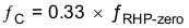
ƒLC ≤ 0.1 ƒRHP
The following requirements for compensating the loop have to be satisfied for the control-to-output gain of a CCM boost operation.

Where:
M = 10 – for tantalum capacitors
M = 15 – for ceramic capacitors
Where:
L = Inductor value,
Co = Output capacitor,
VIN = Input voltage, and
VO = Output voltage
The feed-forward compensation network type 1 is calculated using the pole frequency in Equation 18:
The minimum output capacitor required for a desired output ripple voltage is given by Equation 19:
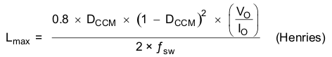
The minimum inductor value needed to ensure CCM from maximum to 25% of maximum load is determined by choosing the value of the inductor to have a ripple current of approximately 40% of the maximum output load current at maximum input voltage of the system.

To maintain ccm operation with at least a 10% of maximum load current (IO-DLM ≥ 0.1 × IO-max) The inductor is given by Equation 21:
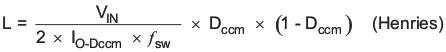
Where:
Dccm = 0.5,
VIN = Typical operating voltage
Choosing an inductor value less than the one determined by Equation 21 may cause the converter to go into DCM operation during low output currents. This may not be a problem if the loop compensation allows for good phase margin.
The ripple current flowing through the output capacitor ESR causes power dissipation in the capacitor. Equation 17 gives the RMS value of the ripple current flowing through the output capacitance.
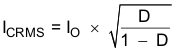
Where:
D = Duty cycle
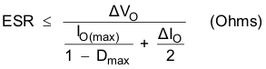
For continuous inductor current mode operation, the ESR needed to limit the ripple voltage ΔVO to volts peak-peak is:
7.4.3 Loop Compensation For Stability Criteria
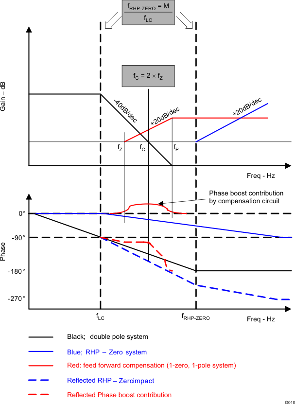 Figure 10. Stability Criteria
Figure 10 is an illustration of stability criteria and is used to ensure converter performance based on the type of loop compensation implemented.