SLVSD05F march 2016 – august 2023 TPS56C215
PRODUCTION DATA
- 1
- 1 Features
- 2 Applications
- 3 Description
- 4 Revision History
- 5 Pin Configuration and Functions
- 6 Specifications
-
7 Detailed Description
- 7.1 Overview
- 7.2 Functional Block Diagram
- 7.3
Feature Description
- 7.3.1 PWM Operation and D-CAP3 Control Mode
- 7.3.2 Eco-mode Control
- 7.3.3 4.7-V LDO
- 7.3.4 MODE Selection
- 7.3.5 Soft Start and Pre-biased Soft Start
- 7.3.6 Enable and Adjustable UVLO
- 7.3.7 Power Good
- 7.3.8 Overcurrent Protection and Undervoltage Protection
- 7.3.9 Out-of-Bounds Operation
- 7.3.10 UVLO Protection
- 7.3.11 Thermal Shutdown
- 7.3.12 Output Voltage Discharge
- 7.4 Device Functional Modes
- 8 Application and Implementation
- 9 Device and Documentation Support
- 10Mechanical, Packaging, and Orderable Information
Package Options
Mechanical Data (Package|Pins)
- RNN|18
Thermal pad, mechanical data (Package|Pins)
Orderable Information
7.3.6 Enable and Adjustable UVLO
The EN pin controls the turnon and turnoff of the device. When EN pin voltage is above the turnon threshold which is around 1.2 V, the device starts switching and when the EN pin voltage falls below the turnoff threshold, which is around 1.1 V, it stops switching. If the user application requires a different turnon (VSTART) and turnoff thresholds (VSTOP) respectively, the EN pin can be configured as shown in Figure 7-3 by connecting a resistor divider between VIN and EN. The EN pin has a pullup current Ip1 that sets the default state of the pin when it is floating. This current increases to Ip2 when the EN pin voltage crosses the turnon threshold. The UVLO thresholds can be set by using Equation 4 and Equation 5.
 Figure 7-3 Adjustable VIN Undervoltage Lock Out
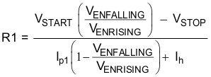
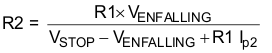
where
- Ip2 = 4.197 μA
- Ip1 = 1.91 μA
- Ih = 2.287 μA
- VENRISING = 1.225 V
- VENFALLING = 1.104 V