SLUS525A March 2007 – September 2015 TPS61050 , TPS61052
PRODUCTION DATA.
- 1 Features
- 2 Applications
- 3 Description
- 4 Revision History
- 5 Pin Configuration and Functions
- 6 Specifications
- 7 Detailed Description
-
8 Application and Implementation
- 8.1 Application Information
- 8.2
Typical Applications
- 8.2.1 Typical Application Schematic
- 8.2.2 High-Power White LED Solution Featuring Privacy Indicator
- 8.2.3 High-Power White LED Solution Featuring No-Latency Turn-Down Through PA TX Signal
- 8.2.4 High-Power White LED Flash Driver And AF/Zoom Motor Drive Supply
- 8.2.5 White LED Flash Driver and Audio Amplifier Power Supply Exclusive Operation
- 8.2.6 White LED Flash Driver and Audio Amplifier Power Supply Operating Simultaneously
- 8.2.7 White LED Flash Driver and Auxiliary Lighting Zone Power Supply
- 8.2.8 2 × 300 mA Dual LED Camera Flash
- 9 Power Supply Recommendations
- 10Layout
- 11Device and Documentation Support
- 12Mechanical, Packaging, and Orderable Information
Package Options
Mechanical Data (Package|Pins)
Thermal pad, mechanical data (Package|Pins)
- DRC|10
Orderable Information
12 Mechanical, Packaging, and Orderable Information
The following pages include mechanical, packaging, and orderable information. This information is the most current data available for the designated devices. This data is subject to change without notice and revision of this document. For browser-based versions of this data sheet, refer to the left-hand navigation.
12.1 Package Summary
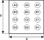
 Figure 64. Chip Scale Package (Bottom View)
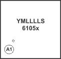
 Figure 65. Chip Scale Package (Top View)
Code:
- Y — 2 digit date code
- LLLL - lot trace code
- S - assembly site code