SLUS525A March 2007 – September 2015 TPS61050 , TPS61052
PRODUCTION DATA.
- 1 Features
- 2 Applications
- 3 Description
- 4 Revision History
- 5 Pin Configuration and Functions
- 6 Specifications
- 7 Detailed Description
-
8 Application and Implementation
- 8.1 Application Information
- 8.2
Typical Applications
- 8.2.1 Typical Application Schematic
- 8.2.2 High-Power White LED Solution Featuring Privacy Indicator
- 8.2.3 High-Power White LED Solution Featuring No-Latency Turn-Down Through PA TX Signal
- 8.2.4 High-Power White LED Flash Driver And AF/Zoom Motor Drive Supply
- 8.2.5 White LED Flash Driver and Audio Amplifier Power Supply Exclusive Operation
- 8.2.6 White LED Flash Driver and Audio Amplifier Power Supply Operating Simultaneously
- 8.2.7 White LED Flash Driver and Auxiliary Lighting Zone Power Supply
- 8.2.8 2 × 300 mA Dual LED Camera Flash
- 9 Power Supply Recommendations
- 10Layout
- 11Device and Documentation Support
- 12Mechanical, Packaging, and Orderable Information
Package Options
Mechanical Data (Package|Pins)
Thermal pad, mechanical data (Package|Pins)
- DRC|10
Orderable Information
5 Pin Configuration and Functions
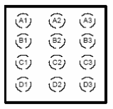
YZG Package
12-Pin DSBGA
Top View

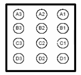
YZG Package
12-Pin DSBGA
Bottom View

Pin Functions
| PIN | I/O | DESCRIPTION | ||
|---|---|---|---|---|
| NAME | VSON | DSBGA | ||
| AVIN | 5 | D3 | I | This is the input voltage pin of the device. Connect directly to the input bypass capacitor. |
| VOUT | 9 | A2 | O | Boost converter output. |
| LED | 6 | D2 | I | LED return input. This feedback pin regulates the LED current through the internal sense resistor by regulating the voltage across it. The regulation operates with typically 250 mV dropout voltage. Connect to the cathode of the LED. |
| FLASH_SYNC | 10 | A1 | I | Flash strobe pulse synchronization input. |
| FLASH_SYNC = LOW (GND): The device is operating and regulating the LED current to the torch current level (TC). | ||||
| FLASH_SYNC = HIGH (VIN): The device is operating and regulating the LED current to the flash current level (FC). | ||||
| SCL | 2 | B3 | I | Serial interface clock line. This pin must not be left floating and must be terminated. |
| SDA | 1 | A3 | I/O | Serial interface address/data line. This pin must not be left floating and must be terminated. |
| GPIO | 3 | C3 | I/O | General purpose input/output (refer to REGISTER2). This pin can either be configured as a logic input or as an open-drain output (TPS61050). |
| ENVM | 3 | C3 | I | Enable pin for voltage mode boost converter (TPS61052). |
| SW | 8 | B1, B2 | I/O | Inductor connection. Drain of the internal power MOSFET. Connect to the switched side of the inductor. SW is high impedance during shutdown. |
| PGND | 7 | C1, C2 | — | Power ground. Connect to AGND underneath IC. |
| AGND | 4 | D1 | — | Analog ground. |
| PowerPAD™ | — | — | — | Internally connected to PGND. |
