SLVS625E February 2006 – November 2015 TPS61150 , TPS61151
PRODUCTION DATA.
- 1 Features
- 2 Applications
- 3 Description
- 4 Revision History
- 5 Device Comparison Tables
- 6 Pin Configuration and Functions
- 7 Specifications
- 8 Detailed Description
- 9 Application and Implementation
- 10Power Supply Recommendations
- 11Layout
- 12Device and Documentation Support
- 13Mechanical, Packaging, and Orderable Information
Package Options
Mechanical Data (Package|Pins)
- DRC|10
Thermal pad, mechanical data (Package|Pins)
- DRC|10
Orderable Information
11 Layout
11.1 Layout Guidelines
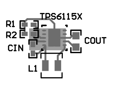
As for all switching power supplies, especially those providing high current and using high switching frequencies, printed circuit board (PCB) layout is an important design step. If layout is not carefully done, the regulator could show instability as well as electromagnetic interference (EMI) problems. Therefore, use wide and short traces for high current paths. The input capacitor must not only be close to the VIN pin, but also to the GND pin in order to reduce the input ripple seen by the device. The VIN and SW pins are conveniently located on the edges of the device; therefore, the inductor can be placed close to the device. The output capacitor must be placed near the load to minimize ripple and maximize transient performance.
It is also beneficial to have the ground of the output capacitor close to the GND pin because there will be a large ground return current flowing between these two connections. When laying out the signal ground, use short traces separated from power ground traces, and connect them together at a single point on the PCB.
11.2 Layout Example
 Figure 18. TPS61150 Layout Example