SLVS625E February 2006 – November 2015 TPS61150 , TPS61151
PRODUCTION DATA.
- 1 Features
- 2 Applications
- 3 Description
- 4 Revision History
- 5 Device Comparison Tables
- 6 Pin Configuration and Functions
- 7 Specifications
- 8 Detailed Description
- 9 Application and Implementation
- 10Power Supply Recommendations
- 11Layout
- 12Device and Documentation Support
- 13Mechanical, Packaging, and Orderable Information
Package Options
Mechanical Data (Package|Pins)
- DRC|10
Thermal pad, mechanical data (Package|Pins)
- DRC|10
Orderable Information
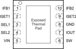
6 Pin Configuration and Functions
DRC Package
10-Pin VSON With Exposed Thermal Pad
Top View

Pin Functions
| PIN | I/O | DESCRIPTION | |
|---|---|---|---|
| NUMBER | NAME | ||
| 1, 10 | IFB1, IFB2 | I | The return path for the IOUT regulation. Current regulator is connected to this pin, and it can be disabled to open the current path. |
| 2, 9 | ISET1, ISET2 | I | Output current programming pins. The resistor connected to the pin programs its corresponding output current. |
| 3, 4 | SEL1, SEL2 | I | Mode selection pins. See Table 2 for details. |
| 5 | VIN | I | The input pin to the device. It provides the current to the boost power stage and also powers the device circuit. When VIN is below the undervoltage lockout threshold, the device turns off and disables outputs, thus disconnecting the WLEDs from the input. |
| 6 | SW | I | This is the switching node of the device. |
| 7 | IOUT | O | The output of the constant current supply. It is directly connected to the boost converter output. |
| 8 | GND | O | The ground of the device. Connect the input and output capacitors very close to this pin. |
| — | Thermal Pad | — | The thermal pad should be soldered to the analog ground. If possible, use thermal via to connect to ground plane for ideal power dissipation. |