SLVSC13A July 2013 – March 2016
PRODUCTION DATA.
- 1 Features
- 2 Applications
- 3 Description
- 4 Revision History
- 5 Device Comparison Table
- 6 Pin Configuration and Function
- 7 Specifications
- 8 Detailed Description
- 9 Application and Implementation
- 10Power Supply Recommendations
- 11Layout
- 12Device and Documentation Support
- 13Mechanical, Packaging, and Orderable Information
Package Options
Mechanical Data (Package|Pins)
- YFF|9
Thermal pad, mechanical data (Package|Pins)
Orderable Information
8 Detailed Description
8.1 Overview
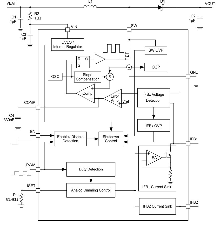
The TPS61162D is a high-efficiency, dual-channel white LED driver for smart-phone backlighting applications. The device operates over the 2.7-V to 6.5-V input voltage range.
The TPS61162D consists of an inductive boost plus two current sink white-LED drivers designed to power one or two LED strings with up to ten LEDs each (up to 26.5 V typical), with a maximum of 30 mA per string. The power for the LED strings comes from an integrated asynchronous backlight boost converter operating at 1.2-MHz switching frequency. LED current is regulated by the low-headroom current sinks. The inductive backlight boost automatically adjusts its output voltage to keep the active current sinks in regulation, while minimizing current sink headroom voltage. Additionally, the TPS61162D includes protection circuits for overcurrent, overvoltage and thermal shutdown protection.
8.2 Functional Block Diagram
8.3 Feature Description
8.3.1 Normal Operation
In order to provide high brightness backlighting for large-sized or high-resolution smart-phone panels, a greater number of white LED diodes are used. Having all LED diodes in a string improves overall current matching; however, the output voltage of a boost converter is limited when input voltage is low, and normally the efficiency drops when the output voltage is very high. For these reasons, the TPS61162D is designed to configure the LED diodes in two parallel strings.
8.3.2 Boost Converter
The boost converter of the TPS61162D integrates a 40-V, 1.5-A low-side switch MOSFET and has a fixed switching frequency of 1.2 MHz. The control architecture is based on traditional current-mode PWM control. (For operation see Functional Block Diagram.) Two current sinks regulate the dual-channel current, and the boost output is automatically set by the voltage of the regulating IFBx pin. The output of the error amplifier and the sensed current of the switch MOSFET are applied to a control comparator to generate the boost switching duty cycle; slope compensation is added to the current signal to allow stable operation for duty cycles larger than 50%.
In order to ensure that both current sinks remain in regulation whenever there is a mismatch in string voltages while the power dissipation of the current sink regulators is minimized, the minimum headroom voltage between IFB1 and IFB2 becomes the regulation point for the boost converter. For example, if the LEDs connected to IFB1 require 20 V, and the LEDs connected to IFB2 require 20.5 V at the programmed current, then the voltage at IFB2 is about 90 mV, and the voltage at IFB1 is about 0.59 V. In other words, the boost makes the cathode of the highest voltage LED string the regulation point.
8.3.3 IFBx Pin Unused
If only one channel is needed, a user can easily disable the unused channel by connecting its IFBx pin to ground. If both IFBx pins are connected to ground, the device does not start up.
8.3.4 Enable and Start-Up
In order to enable the device from shutdown mode, three conditions have to be met:
- Power On Reset (POR), that is, VIN voltage is higher than UVLO threshold
- Logic high on EN pin
- PWM signal (logic high or PWM pulses) on PWM pin
The TPS61162D supports two dimming interfaces: one-wire digital interface (EasyScale interface) and PWM interface. The device begins an EasyScale detection window after start-up to detect which interface is selected. If the EasyScale interface is needed, signals of a specific pattern must be input into the EN pin during the EasyScale detection window; otherwise, PWM dimming interface is enabled (see details in One-Wire Digital Interface (Easyscale Interface)).
After the EasyScale detection window, the TPS61162D checks the status of IFBx pins. If one IFBx pin is detected to connect to ground, the corresponding channel is disabled and removed from the control loop. The soft start then begins, and the boost converter starts switching. If both IFBx pins are shorted to ground, the TPS61162D does not start up.
Either pulling EN pin low for more than 2.5 ms, or pulling the PWM pin low for more than 20 ms, can disable the device, and the TPS61162D enters into shutdown mode.
8.3.5 Soft Start
Soft start is implemented internally to prevent voltage overshoot and inrush current. After the IFBx pin status detection, the COMP pin voltage starts ramp up, and the boost starts switching. During the beginning 5 ms (tHalf_LIM) of the switching, the peak current of the switch MOSFET is limited at ILIM_Start (0.7 A typical) to prevent excess inrush input current. After 5 ms the current limit is changed to ILIM (1.5 A typical) to allow the normal operation of the boost converter.
8.3.6 Full-Scale Current Program
The dual channels of the TPS61162D can provide up to 30 mA current each — when either the EasyScale interface or PWM interface is selected, the full-scale current (current when dimming duty cycle is 100%) of each channel must be programmed by an external resistor RISET at ISET pin according to Equation 1.

where
- IFB_full = full-scale current of each channel
- KISET_full = 1030 (Current multiple when dimming duty cycle = 100%)
- VISET_full = 1.229 V (ISET pin voltage when dimming duty cycle = 100%)
- RISET = ISET pin resistor
8.3.7 Brightness Control
The TPS61162D controls the DC current of the dual channels to realize the brightness dimming. The DC current control is normally referred to as analog dimming mode. When the DC current of LED diode is reduced, the brightness is dimmed.
The TPS61162D can receive either the PWM signals at the PWM pin (PWM interface) or digital commands at the EN pin (EasyScale interface) for brightness dimming. If the EasyScale interface is selected, the PWM pin must be kept high; if PWM interface is selected, the EN pin must be kept high.
8.3.8 Undervoltage Lockout
An undervoltage lockout circuit prevents the operation of the device at input voltages below undervoltage threshold (2.2 V typical). When the input voltage is below the threshold, the device is shut down. If the input voltage rises by undervoltage lockout hysteresis, the device restarts.
8.3.9 Overvoltage Protection
Overvoltage protection circuitry prevents device damage as the result of white LED string disconnection or shortage.
The TPS61162D monitors the voltages at the SW and IFBx pins during each switching cycle. If either SW OVP threshold VOVP_SW or IFBx OVP threshold VOVP_FB is reached due to the LED string open or short issue, the protection circuitry is triggered. Refer to Figure 6 and Figure 7 for the protection actions.
If one LED string is open, its IFBx pin voltage drops, and the boost output voltage is increased by the control loop as it tries to regulate this lower IFBx voltage to the target value (90 mV typical). The current of the normally operating string is properly regulated but its IFBx voltage rises because of the rise in output voltage. During this process, either the SW voltage reaches the OVP threshold VOVP_SW or the IFBx voltage of the normally operating string reaches its overvoltage threshold VOVP_FB, and the corresponding protection mechanism is triggered.
If both LED strings are open, the voltages of both IFBx pins drop to ground, and the boost output voltage is increased by the control loop until it reaches the SW OVP threshold VOVP_SW. At that point the SW OVP protection circuitry is triggered, and the device is latched off. Only the VIN POR pin or EN/PWM pin toggling can restart the device.
One LED diode short in a string is allowed in the TPS61162D. If one LED diode in a string is short, the IFBx voltage of the normal string is regulated to about 90 mV, and the IFBx pin voltage of the abnormal string is higher. Typically with only one diode short, the higher IFBx pin voltage does not reach the IFBx OVP threshold VOVP_FB, so the protection circuitry is not triggered.
If more than one LED diodes are short in a string, as the boost loop regulates the IFBx normal string voltage to 90 mV, the IFBx pin voltage of the abnormal string is much higher and reaches VOVP_FB — then the protection circuitry is triggered.
SW OVP protection is also triggered when the forward voltage drop of an LED string exceeds the SW OVP threshold. In this case, the device turns off the switch FET and shuts down.
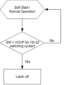 Figure 6. SW OVP Protection Action
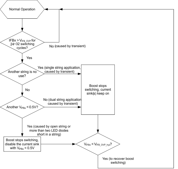 Figure 7. VIFBx OVP Protection Action
8.3.10 Overcurrent Protection
The TPS61162D has a pulse-by-pulse overcurrent limit. The boost switch turns off when the inductor current reaches this current threshold, and it remains off until the beginning of the next switching cycle. This protects the TPS61162D and external components under overload conditions.
8.3.11 Thermal Shutdown
An internal thermal shutdown turns off the device when the typical junction temperature of 160°C is exceeded. The device is released from shutdown automatically when the junction temperature decreases by 15°C.
8.4 Device Functional Modes
8.4.1 One-Wire Digital Interface (Easyscale Interface)
The EN pin features a simple digital interface to allow digital brightness control. The digital dimming interface can save the processor power and battery life as it does not require PWM signals all the time, and the processor can enter idle mode if possible. In order to enable the EasyScale interface, the following conditions must be satisfied, and the specific digital pattern on the EN pin must be recognized by the device every time the TPS61162D starts up from shutdown mode:
- VIN voltage is higher than UVLO threshold and PWM pin is pulled high.
- Pull the EN pin from low to high to enable the TPS61162D. At this moment, the EasyScale detection window starts.
- After EasyScale detection delay time (tes_delay = 100 µs), drive EN to low for greater than EasyScale detection time (tes_detect = 260 µs).
The third step must be finished before the EasyScale detection window (tes_win = 1 ms) expires; once this step is finished, the EasyScale interface is enabled, and the EasyScale communication can start. Refer to the Figure 8 for a graphical explanation.
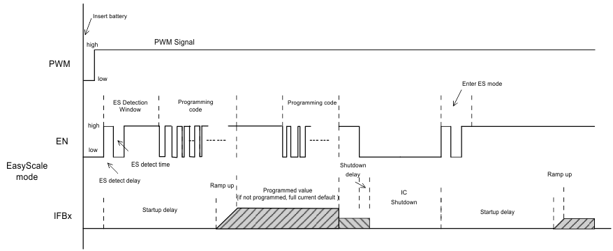 Figure 8. EasyScale Interface Detection
The TPS61162D supports 9-bit brightness code programming. Using the EasyScale interface, a master can program the 9-bit code D8(MSB) to D0(LSB) to any of 511 steps with a single command. The default code value of D8 to D0 is 111111111 when the device is first enabled, and the programmed value is stored in an internal register and set the dual-channel current according to Equation 2. The code is reset to default value when the device is shut down or disabled.

where
- IFB_full = the full-scale LED current set by the RISET at ISET pin
- Code = the 9-bit brightness code D8 - D0 programmed by the EasyScale interface
When the one-wire digital interface at EN pin is selected, the PWM pin can be connected to either the VIN pin or a GPIO (refer to Additional Application Circuits). If the PWM pin is connected to the VIN pin, the EN pin alone can enable and disable the device:
- Pulling the EN pin low for more than 2.5 ms disables the device.
- If the PWM pin is connected to a GPIO, both PWM and EN signals must be high to enable the device.
- Either pulling EN pin low for more than 2.5 ms or pulling PWM pin low for more than 20 ms disables the device.
8.4.2 PWM Control Interface
The PWM control interface is automatically enabled if the EasyScale interface fails to be enabled during start-up. In this case, the TPS61162D receives PWM dimming signals on the PWM pin to control the backlight brightness. When using PWM interface, the EN pin can be connected to the VIN pin or a GPIO (refer to Additional Application Circuits). If the EN pin is connected to the VIN pin, the PWM pin alone is used to enable and disable the device; applying a signal at the PWM pin enables the device; pulling the PWM pin low for more than 20 ms disables the device; if the EN pin is connected to a GPIO, either pulling the EN pin low for more than 2.5 ms or pulling the PWM pin low for more than 20 ms disables the device. Only after both EN and PWM signals are applied can the TPS61162D start up (see Figure 9).
 Figure 9. PWM Control Interface Detection
When the PWM pin is constantly high, the dual channel current is regulated to full scale according to Equation 1. The PWM pin allows PWM signals to reduce this regulation current according to the PWM duty cycle; therefore, it achieves LED brightness dimming. The relationship between the PWM duty cycle and the IFBx current is given by Equation 3.

where
- IFBx = the current of each current sink
- IFB_full = the full-scale LED current
- Duty = the duty cycle information detected from the PWM signals
8.5 Programming
8.5.1 EasyScale Programming
EasyScale is a simple and flexible one-pin interface used to configure the current of the dual channels. The interface is based on a master-slave structure, where the master is typically a microcontroller or application processor and the device is the slave. Figure 10 and Table 1 give an overview of the protocol used by TPS61162D. A command consists of 24 bits, including an 8-bit device address byte and a 16-bit data byte. All 24 bits must be transmitted together each time, and the LSB bit must be transmitted first. The device address byte D7(MSB) to D0(LSB) is fixed to 0x8F. The data byte includes 9 bits D8(MSB) to D0(LSB) for brightness information and an RFA bit. The RFA bit set to 1 indicates the Request for Acknowledge condition. The Acknowledge condition is only applied when the protocol is received correctly. The advantage of EasyScale compared with other one-pin interfaces is that its bit detection is, to a large extent, independent from the bit transmission rate. EasyScale can automatically detect bit rates from 1.7 kBit/second up to 160 kBit/second.
 Figure 10. EasyScale Protocol Overview
Table 1. EasyScale Bit Description
| BYTE | BIT NUMBER | NAME | TRANSMISSION DIRECTION | DESCRIPTION |
|---|---|---|---|---|
| Device Address Byte (0x8F) | 23 (MSB) | DA7 | IN | DA7 = 1, MSB of device address |
| 22 | DA6 | DA6 = 0 | ||
| 21 | DA5 | DA5 = 0 | ||
| 20 | DA4 | DA4 = 0 | ||
| 19 | DA3 | DA3 = 1 | ||
| 18 | DA2 | DA2 = 1 | ||
| 17 | DA1 | DA1 = 1 | ||
| 16 | DA0 | DA0 = 1, LSB of device address | ||
| Data Byte | 15 | Bit 15 | IN | No information. Write 0 to this bit. |
| 14 | Bit 14 | No information. Write 0 to this bit. | ||
| 13 | Bit 13 | No information. Write 0 to this bit. | ||
| 12 | Bit 12 | No information. Write 0 to this bit. | ||
| 11 | Bit 11 | No information. Write 0 to this bit. | ||
| 10 | RFA | Request for acknowledge. If set to 1, the device pulls low the data line when it receives the command well. This feature can only be used when the master has an open drain output stage and the data line needs to be pulled high by the master with a pullup resistor; otherwise, acknowledge condition is not allowed and don't set this bit to 1. | ||
| 9 | Bit 9 | No information. Write 0 to this bit. | ||
| 8 | D8 | Data bit 8, MSB of brightness code | ||
| 7 | D7 | Data bit 7 | ||
| 6 | D6 | Data bit 6 | ||
| 5 | D5 | Data bit 5 | ||
| 4 | D4 | Data bit 4 | ||
| 3 | D3 | Data bit 3 | ||
| 2 | D2 | Data bit 2 | ||
| 1 | D1 | Data bit 1 | ||
| 0 (LSB) | D0 | Data bit 0, LSB of brightness code |
 Figure 11. EasyScale Timing With RFA = 0
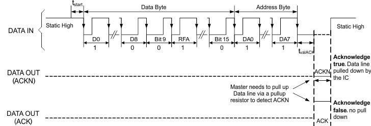 Figure 12. EasyScale Timing With RFA = 1
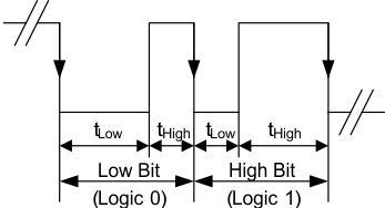 Figure 13. Easyscale — Bit Coding
The 24-bit command must be transmitted with LSB first and MSB last. Figure 11 shows the protocol without acknowledge request (Bit RFA = 0), Figure 12 with acknowledge request (Bit RFA = 1). Before the command transmission, a start condition must be applied. For this, the EN pin must be pulled high for at least tstart (2 μs) before the bit transmission starts with the falling edge. If the EN pin is already at high level, no start condition is needed. The transmission of each command is closed with an End of Stream condition for at least tEOS (2 μs).
The bit detection is based on a Logic Detection scheme, where the criterion is the relation between tLOW and tHIGH (refer to Figure 13). It can be simplified to:
Low Bit (Logic 0): tLOW ≥ 2 × tHIGH
High Bit (Logic 1): tHIGH ≥ 2 × tLOW
The bit detection starts with a falling edge on the EN pin and ends with the next falling edge. Depending on the relation between tHIGH and tLOW, the logic 0 or 1 is detected.
The acknowledge condition is only applied if:
- Acknowledge is requested by setting RFA bit to 1.
- The transmitted device address matches with the device address of the device.
- A total of 24 bits are received correctly.
If above conditions are met, after tvalACK delay from the moment when the last falling edge of the protocol is detected, an internal ACKN-MOSFET is turned on to pull the EN pin low for the time tACKN, which is 512 μs maximum, then the acknowledge condition is valid. During the tvalACK delay, the master controller keeps the line low; after the delay, it must release the line by outputting high impedance and then detect the acknowledge condition. If it reads back a logic 0, the device has received the command correctly. The EN pin can be used again by the master when the acknowledge condition ends after tACKN time.
Note that the acknowledge condition can only be requested when the master device has an open drain output. For a push-pull output stage, the use of a series resistor in the EN line to limit the current to 500 μA is recommended to for such cases as:
- An accidentally requested acknowledge, or
- To protect the internal ACKN-MOSFET.