SLVSC13A July 2013 – March 2016
PRODUCTION DATA.
- 1 Features
- 2 Applications
- 3 Description
- 4 Revision History
- 5 Device Comparison Table
- 6 Pin Configuration and Function
- 7 Specifications
- 8 Detailed Description
- 9 Application and Implementation
- 10Power Supply Recommendations
- 11Layout
- 12Device and Documentation Support
- 13Mechanical, Packaging, and Orderable Information
Package Options
Mechanical Data (Package|Pins)
- YFF|9
Thermal pad, mechanical data (Package|Pins)
Orderable Information
11 Layout
11.1 Layout Guidelines
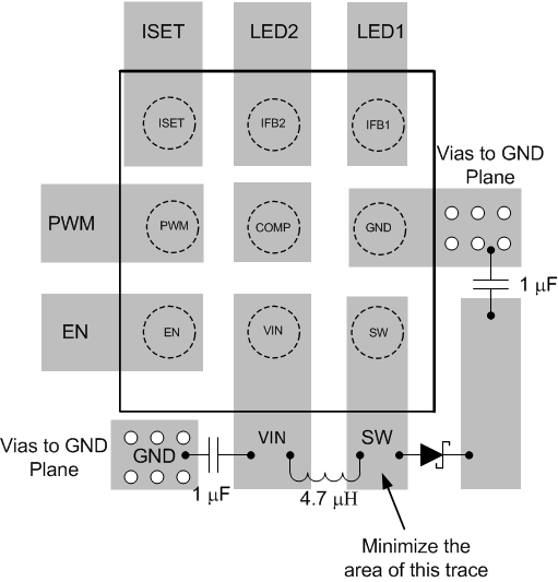
As for all switching power supplies, especially those providing high current and using high switching frequencies, layout is an important design step. If layout is not carefully done, the regulator could show instability as well as EMI problems. Therefore, use wide and short traces for high current paths. The input capacitor, C1 in the Figure 14, must be close to the inductor, as well as the VIN and GND pins, in order to reduce the input ripple detected by the device. If possible, choose a higher capacitance value for C1. If the ripple seen at VIN pin is so great that it affects the boost loop stability or internal circuits operation, TI recommends R2 and C3 to filter and decouple the noise. In this case, C3 must be placed as close to the VIN and GND pins as possible.
The SW pin carries high current with fast rising and falling edges. Therefore, the connection between the SW pin to the inductor and Schottky diode must be kept as short and wide as possible. The trace between the Schottky diode and the output capacitor C2 must also be as short and wide as possible. It is beneficial to have the ground of the output capacitor C2 close to the GND pin because there is a large ground return current flowing between them. When laying out signal grounds, TI recommends using short traces separated from power ground traces, and connecting them together at a single point close to the GND pin.
11.2 Layout Example
 Figure 24. TPS61162D Layout Example