SNVSA76B March 2015 – March 2017 TPS61177A
PRODUCTION DATA.
- 1 Features
- 2 Applications
- 3 Description
- 4 Revision History
- 5 Pin Configuration and Functions
- 6 Specifications
-
7 Detailed Description
- 7.1 Overview
- 7.2 Functional Block Diagram
- 7.3
Feature Description
- 7.3.1 Supply Voltage
- 7.3.2 Boost Regulator
- 7.3.3 Programmable Switch Frequency and Slew Rate
- 7.3.4 LED Current Sinks
- 7.3.5 Enable and Start-Up Timing
- 7.3.6 Input Undervoltage Protection (UVLO)
- 7.3.7 Overvoltage Protection (OVP)
- 7.3.8 Current-Sink Open Protection
- 7.3.9 Overcurrent Protection
- 7.3.10 Thermal Protection
- 7.4 Device Functional Modes
- 7.5 Programming
- 7.6
Register Maps
- 7.6.1 MODE (A0h)
- 7.6.2 CS (A1h)
- 7.6.3 UVLO (A2h)
- 7.6.4 FREQ (A3h)
- 7.6.5 SR (A4h)
- 7.6.6 ILIM (A5h)
- 7.6.7 Control (FFh)
- 7.6.8 Example - Writing to a Single RAM Register
- 7.6.9 Example - Writing to Multiple RAM Registers
- 7.6.10 Example - Saving Contents of all RAM Registers to E2PROM
- 7.6.11 Example - Reading from a Single RAM Register
- 7.6.12 Example - Reading from a Single E2PROM Register
- 7.6.13 Example - Reading from Multiple RAM Registers
- 7.6.14 Example - Reading from Multiple E2PROM Registers
- 8 Application and Implementation
- 9 Power Supply Recommendations
- 10Layout
- 11Device and Documentation Support
- 12Mechanical, Packaging, and Orderable Information
Package Options
Mechanical Data (Package|Pins)
- RGR|20
Thermal pad, mechanical data (Package|Pins)
- RGR|20
Orderable Information
8 Application and Implementation
NOTE
Information in the following applications sections is not part of the TI component specification, and TI does not warrant its accuracy or completeness. TI’s customers are responsible for determining suitability of components for their purposes. Customers should validate and test their design implementation to confirm system functionality.
8.1 Application Information
8.1.1 CS Pin Unused
The TPS61177A has open/short string detection. For an unused CS string, simply short it to ground or leave it open. If the CS pin is open, the boost output voltage ramps up to overvoltage threshold during start-up. The device then detects the zero current string and removes it from the feedback loop. If the CS pin is shorted to ground, the device detects the short and immediately removes it (or them) out of feedback loop within 4 ms after device enable, and the boost output voltage does not go up to overvoltage threshold. Instead, it ramps to the regulation voltage after soft start.
Shorting unused CS pins to ground for faster start-up is recommended.
8.1.2 Brightness Dimming Control
The TPS61177A has three dimming methods. See Mode Selection section for dimming mode selection. With analog and PWM mixed dimming or pure analog dimming through the PWM control interface, the internal decoder block detects duty information from the input PWM signal, saves it in an up to 10-bits register and delivers to either a mixed mode dimming control circuit or pure analog dimming control circuit. In mixed dimming mode, the output dimming control circuit sets the DC current of six current sinks linearly between 25% and 100% at same scale to the value in up to a 10-bits register. When the brightness level is below 25% to full-scale value, the dimming control circuit turns on/off six output current sinks at same frequency with PWMB and duty cycle out of shift register. See Analog and PWM Mixed Dimming Mode section for more explanation. While in pure analog dimming mode, the output dimming control circuit sets the DC current of six current sinks linearly between 1% and 100% at same scale to the value in up to a 10-bits register. See Analog Dimming Mode section for more detail explanation.
The TPS61177A also has direct PWM dimming control through the PWM control interface. In direct PWM mode, each current sink turns on/off at the same frequency and duty cycle as the input PWM signal. See Direct PWM Dimming section for more explanation.
When in analog and PWM mixed mode, insertion of a series 10-kΩ to 20-kΩ resistor close to PWMB pin is recommended. This resistor, together with an internal capacitor, forms a low pass R-C filter with a 30-ns to 60-ns time constant. This prevents possible high frequency noise being coupled into the input PWM signal and causing interference to the internal duty cycle decoding circuit. However, it is not necessary for direct PWM mode since the duty cycle decoding circuit is disabled during direct PWM mode.
8.2 Typical Application
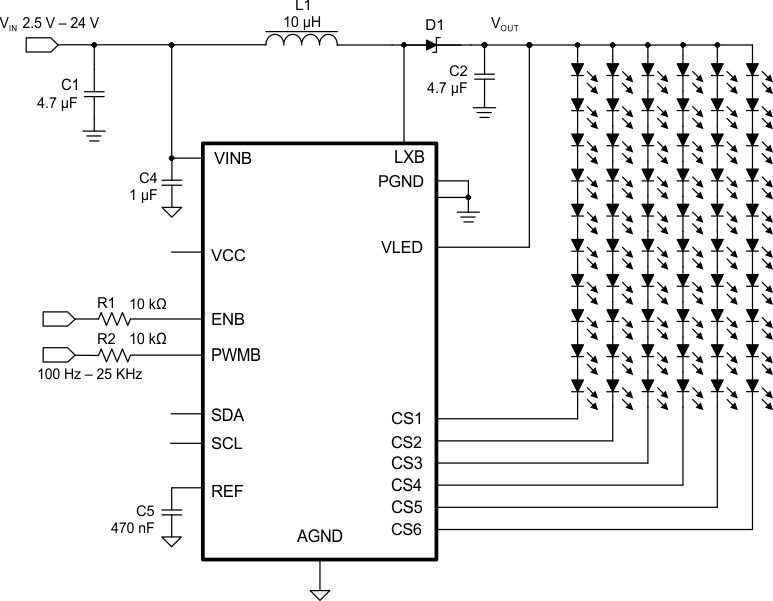
 Figure 36. TPS61177A Typical Application
8.2.1 Design Requirements
| DESIGN PARAMETER | EXAMPLE VALUE |
|---|---|
| Inductor | 10 µH |
| Minimum input voltage | 2.5 V |
| Number of series LED | 12 |
| LED maximum forward voltage (Vf) | 3.3 V |
| Schottky diode forward voltage (Vf) | 0.2 V |
| Efficiency (η) | 85% |
| Switching frequency | 600 kHz |
| PWM input frequency | 1 kHz |
| Maximum LED string current | 30 mA |
The TPS61177A is designed to support up to 2.2 A (typical) SW current. Thus, SW current must be carefully calculated with factors such as inductor, target efficiency, output voltage, load current, and so forth. In most cases, the voltage ratio between input and boost output must be < 10.
8.2.2 Detailed Design Procedure
8.2.2.1 Inductor Selection
Because selection of the inductor affects power supply steady-state operation, transient behavior, and loop stability, the inductor is the most important component in switching power regulator design. There are three specifications most important to the performance of the inductor: inductor value, DC resistance, and saturation current. The TPS61177A is designed to work with inductor values between 4.7 µH and 22 µH. A 10-µH inductor is typically available in a smaller or lower profile package, while a 22-µH inductor may produce higher efficiency due to a slower switching frequency and/or lower inductor ripple. If the boost output current is limited by the overcurrent protection of the device, using a 10-µH inductor and the highest switching frequency maximizes controller output current capability.
Internal loop compensation for PWM control is optimized for the external component values, including typical tolerances, recommended in Table 10. Inductor values can have ±20% tolerance with no current bias. When the inductor current approaches saturation level, its inductance can decrease 20% to 35% from the 0-A value depending on how the inductor vendor defines saturation. In a boost regulator, the inductor DC current can be calculated with Equation 1.

where
- VOUT = boost output voltage
- IOUT = boost output current
- VIN = boost input voltage
- η = power conversion efficiency, use 90% for TPS61177A applications
The inductor current peak-to-peak ripple can be calculated with Equation 2.

where
- ΔIL(P-P) = inductor peak-to-peak ripple
- L = inductor value
- FS = Switching frequency
- VOUT = boost output voltage
- VIN = boost input voltage
Therefore, the peak current seen by the inductor is calculated with Equation 3.

Select an inductor with a saturation current over the calculated peak current. To calculate the worst-case inductor peak current, use the minimum input voltage, maximum output voltage, and maximum load current.
Regulator efficiency is dependent on the resistance of its high current path and switching losses associated with the power FET switch and power diode. Although the TPS61177A device has optimized the internal switch resistances, the overall efficiency is affected by the inductor DC resistance (DCR). Lower DCR improves efficiency. However, there is a trade off between DCR and inductor footprint; furthermore, shielded inductors typically have higher DCR than unshielded ones. Table 10 lists the recommended inductors.
Table 10. Recommended Inductor
| L (µH) | DCR (mΩ) | ISAT (A) | Size (L × W × H mm) | |
|---|---|---|---|---|
| Cyntec | ||||
| PCMB051H-100MS | 10 | 140 | 3 | 5.4 × 5.2 × 1.6 |
| Taiyo | ||||
| NRA6012T 100ME | 10 | 335 | 1.45 | 6 × 6 × 1.2 |
8.2.2.2 Output Capacitor Selection
The output capacitor is mainly selected to meet the requirement for output ripple and loop stability. This ripple voltage is related to the capacitance of the capacitor and its equivalent series resistance (ESR). Assuming a capacitor with zero ESR, the minimum capacitance needed for a given ripple can be calculated with Equation 4:

where
- Vripple = peak-to-peak output ripple.
The additional part of the ripple caused by ESR is calculated using: Vripple_ESR = IOUT × RESR
Due to its low ESR, Vripple_ESR can be neglected for ceramic capacitors, but must be considered if tantalum or electrolytic capacitors are used. The controller output voltage also ripples due to the load transient that occurs during PWM dimming. The TPS61177A adopts a patented technology to limit this type of output ripple even with the minimum recommended output capacitance. In a typical application, the output ripple is less than 250 mV during PWM dimming with a 4.7-µF output capacitor. However, the output ripple decreases with higher output capacitances.
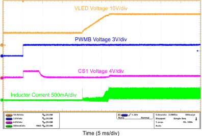
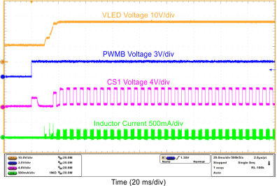
8.2.3 Application Curves

