SNVSA76B March 2015 – March 2017 TPS61177A
PRODUCTION DATA.
- 1 Features
- 2 Applications
- 3 Description
- 4 Revision History
- 5 Pin Configuration and Functions
- 6 Specifications
-
7 Detailed Description
- 7.1 Overview
- 7.2 Functional Block Diagram
- 7.3
Feature Description
- 7.3.1 Supply Voltage
- 7.3.2 Boost Regulator
- 7.3.3 Programmable Switch Frequency and Slew Rate
- 7.3.4 LED Current Sinks
- 7.3.5 Enable and Start-Up Timing
- 7.3.6 Input Undervoltage Protection (UVLO)
- 7.3.7 Overvoltage Protection (OVP)
- 7.3.8 Current-Sink Open Protection
- 7.3.9 Overcurrent Protection
- 7.3.10 Thermal Protection
- 7.4 Device Functional Modes
- 7.5 Programming
- 7.6
Register Maps
- 7.6.1 MODE (A0h)
- 7.6.2 CS (A1h)
- 7.6.3 UVLO (A2h)
- 7.6.4 FREQ (A3h)
- 7.6.5 SR (A4h)
- 7.6.6 ILIM (A5h)
- 7.6.7 Control (FFh)
- 7.6.8 Example - Writing to a Single RAM Register
- 7.6.9 Example - Writing to Multiple RAM Registers
- 7.6.10 Example - Saving Contents of all RAM Registers to E2PROM
- 7.6.11 Example - Reading from a Single RAM Register
- 7.6.12 Example - Reading from a Single E2PROM Register
- 7.6.13 Example - Reading from Multiple RAM Registers
- 7.6.14 Example - Reading from Multiple E2PROM Registers
- 8 Application and Implementation
- 9 Power Supply Recommendations
- 10Layout
- 11Device and Documentation Support
- 12Mechanical, Packaging, and Orderable Information
Package Options
Mechanical Data (Package|Pins)
- RGR|20
Thermal pad, mechanical data (Package|Pins)
- RGR|20
Orderable Information
6 Specifications
6.1 Absolute Maximum Ratings
over operating free-air temperature range (unless otherwise noted) (1)| MIN | MAX | UNIT | ||
|---|---|---|---|---|
| Voltage(2) | VINB | –0.3 | 26.4 | V |
| LXB, VLED, CS1, CS2, CS3, CS4, CS5, CS6 | –0.3 | 40 | ||
| ENB, PWMB | –0.3 | 30 | ||
| SDA, SCL, VCC | –0.3 | 3.6 | ||
| Continuous power dissipation | See Thermal Information | °C | ||
| Operating junction temperature | –40 | 150 | ||
| Storage temperature, Tstg | –65 | 150 | ||
(1) Stresses beyond those listed under Absolute Maximum Ratings may cause permanent damage to the device. These are stress ratings only, which do not imply functional operation of the device at these or any other conditions beyond those indicated under Recommended Operating Conditions. Exposure to absolute-maximum-rated conditions for extended periods may affect device reliability.
(2) All voltage values are with respect to network ground terminal.
6.2 ESD Ratings
| VALUE | UNIT | |||
|---|---|---|---|---|
| V(ESD) | Electrostatic discharge | Human-body model (HBM), per ANSI/ESDA/JEDEC JS-001(1) | ±2000 | V |
| Charged-device model (CDM), per JEDEC specification JESD22-C101(2) | ±1000 | |||
(1) JEDEC document JEP155 states that 500-V HBM allows safe manufacturing with a standard ESD control process.
(2) JEDEC document JEP157 states that 250-V CDM allows safe manufacturing with a standard ESD control process.
6.3 Recommended Operating Conditions
over operating free-air temperature range (unless otherwise noted)| MIN | MAX | UNIT | ||
|---|---|---|---|---|
| VIN | Input voltage | 2.5 | 24 | V |
| VOUT | Output voltage | VIN + 2 | 39 | |
| FPWM_I | PWM input signal frequency | 0.1 | 25 | kHz |
| DMIN_I | PWM input signal minimum duty cycle | 1% | ||
| FBOOST | Boost regulator switching frequency | 450 | 1200 | kHz |
| TA | Operating free-air temperature | –40 | 85 | °C |
| TJ | Operating junction temperature | –40 | 125 | |
6.4 Thermal Information
| THERMAL METRIC(1) | TPS61177A | UNIT | |
|---|---|---|---|
| RGR (VQFN) | |||
| 20 PINS | |||
| RθJA | Junction-to-ambient thermal resistance | 34.4 | °C/W |
| RθJC(top) | Junction-to-case (top) thermal resistance | 46.8 | °C/W |
| RθJB | Junction-to-board thermal resistance | 12.2 | °C/W |
| ψJT | Junction-to-top characterization parameter | 0.5 | °C/W |
| ψJB | Junction-to-board characterization parameter | 12.3 | °C/W |
| RθJC(bot) | Junction-to-case (bottom) thermal resistance | 1.0 | °C/W |
(1) For more information about traditional and new thermal metrics, see the Semiconductor and IC Package Thermal Metrics application report, SPRA953.
6.5 Electrical Characteristics
VINB = 12 V, PWMB/ENB = logic high, CS current = 20 mA, CS voltage = 500 mV, TA = –40°C to +85°C, typical values are at TA = 25°C (unless otherwise noted).| PARAMETER | TEST CONDITIONS | MIN | TYP | MAX | UNIT | |
|---|---|---|---|---|---|---|
| SUPPLY CURRENT | ||||||
| VINB | Input voltage range | 2.5 | 24 | V | ||
| Iq_VINB | Operating quiescent current into VIN | Device enable, no switching and no load, VINB = 12 V |
3.5 | mA | ||
| ISD | Shutdown current | VINB = 12 V, EN = low | 10 | µA | ||
| VINB = 24 V, EN = low | 15 | |||||
| VINB_UVLO | VINB undervoltage lockout threshold, voltage ramp up |
UVLO = 000 | 2.1 | 2.25 | 2.4 | V |
| UVLO = 001 | 2.4 | 2.55 | 2.7 | |||
| UVLO = 010 | 2.8 | 3 | 3.2 | |||
| UVLO = 011 | 3.3 | 3.5 | 3.7 | |||
| Other case | 3.8 | 4 | 4.2 | |||
| VIN_Hys | VIN undervoltage lockout hysteresis | 200 | mV | |||
| BOOST OUTPUT REGULATION | ||||||
| VCS | CS voltage regulation | 500 | 600 | mV | ||
| RDS(ON) | Switch FET on-resistance | VIN = 12 V | 0.20 | 0.35 | Ω | |
| VIN = 3.3 V | 0.30 | 0.40 | ||||
| ILIM | Switching MOSFET current limit | D = Dmax | 1.8 | 2.2 | 2.6 | A |
| ILEAK_LX | Switch FET leakage current | VSW = 40 V | 5 | µA | ||
| FLX | Switching frequency | FREQ = 00 | 0.36 | 0.45 | 0.54 | MHz |
| FREQ = 01 | 0.48 | 0.6 | 0.72 | |||
| FREQ = 10 | 0.64 | 0.8 | 0.96 | |||
| FREQ = 11 | 0.96 | 1.2 | 1.44 | |||
| DMAX | Maximum duty cycle | FLX = 0.8 MHz | 90% | 95% | ||
| TF | Slew rate of switching FET ON | SR = 00 | 4.6 | V/ns | ||
| SR = 01 | 3.5 | |||||
| SR = 10 | 2.5 | |||||
| SR = 11 | 1.3 | |||||
| CS CURRENT REGULATION | ||||||
| ICS | CSn current (See Figure 23) |
ICS = 0000 | 15 | mA | ||
| ICS = 0001 | 16 | |||||
| … | … | |||||
| ICS = 1111 | 30 | |||||
| ICSA | CSn current accuracy (ICSn – 20 mA × DPWM_I)/20 mA x DPWM_I |
ICS = 20 mA, MODE = 00 and 01 DPWM_I = 100%, TA = 25°C |
–3% | 3% | ||
| ICS = 20 mA, MODE = 01 DPWM_I = 255/1023, TA = 25°C |
–3% | 3% | ||||
| ICS = 20 mA, MODE = 10, DPWM_I = 255/1023, TA = 25°C |
–3% | 3% | ||||
| ICS = 20 mA, MODE = 10, DPWM_I = 51/1023, TA = 25°C |
–5% | 5% | ||||
| ICS = 20 mA, MODE = 10, DPWM_I = 10/1023, TA = 25°C |
–8% | 8% | ||||
| ICSM | Current matching (ICSn – IAVG)/IAVG | ICS = 20 mA, MODE = 00 and 01, DPWM_I = 100%, TA = 25°C |
–2% | 2% | ||
| ICS = 20 mA, MODE = 01, DPWM_I = 255/1023, TA = 25°C |
–2% | 2% | ||||
| ICS = 20 mA, MODE = 10, DPWM_I = 255/1023, TA = 25°C |
–2% | 2% | ||||
| ICS = 20 mA, MODE = 10, DPWM_I = 51/1023, TA = 25°C |
–5% | -5% | ||||
| ICS = 20 mA, MODE = 10, DPWM_I = 10/1023, TA = 25°C |
–5% | 5% | ||||
| DC dimming resolution steps | MODE = 01 and 10, FPWM_I = 0.1 to 5 kHz | 1024 | ||||
| MODE = 01 and 10, FPWM_I = 5 to 10 kHz | 512 | |||||
| MODE = 01 and 10, FPWM_I = 10 to 25 kHz | 256 | |||||
| Brightness response time | DPWM_I 10% to 90% MODE = mixed and DC, FPWM_I = 25 kHz |
400 | μs | |||
| DPWM_I 10% to 90% MODE = mixed and DC, FPWM_I = 100 Hz |
10.4 | ms | ||||
| ICSLK | CSn leakage current | VCS = 40 V | 5 | μA | ||
| ICSIR | CSn current inrush | 10% | ||||
| tMP | Minimum dimming pulse | MODE = 00 | 400 | ns | ||
| tDEG | Deglitch pulse width | 125 | ns | |||
| CONTROL AND PROTECTION | ||||||
| VH | ENB logic high threshold | VINB = 2.7 V and 3.3 V | 1.8 | V | ||
| VL | ENB logic low threshold | VINB = 2.7 V and 3.3 V | 0.5 | |||
| VH | PWMB logic high threshold | VINB = 2.7 V and 3.3 V | 1.8 | |||
| VL | PWMB logic low threshold | VINB = 2.7 V and 3.3 V | 0.5 | |||
| RPD | Pulldown resistor on ENB | ENB = 3.3 V | 300 | 600 | 1200 | kΩ |
| Pulldown resistor on PWMB | PWMB = 3.3 V | 300 | 600 | 1200 | ||
| VOVP | Output overvoltage threshold | 39 | 39.5 | 40 | V | |
| Tshutdown | Thermal shutdown threshold | 150 | °C | |||
| Thermal shutdown hysteresis | 15 | |||||
| FSAMPLE | Input sampling oscillator frequency | 22 | 25 | 29 | MHz | |
6.6 I2C Timing Requirements
| MIN | NOM | MAX | UNIT | |||
|---|---|---|---|---|---|---|
| ADDR | Configuration parameters slave address | Write | 58h | |||
| Read | 59h | |||||
| VIL | Low level input voltage | Supply = 2.5 V, VIN falling, standard and fast modes |
0.75 | V | ||
| VIH | High level input voltage | Supply = 2.5 V, VIN rising, standard and fast modes |
1.75 | V | ||
| VHYS | Hysteresis | Supply = 2.5 V, applicable to fast mode only |
125 | mV | ||
| VOL | Low level output voltage | Sinking 3 mA | 500 | mV | ||
| CI | Input capacitance | 10 | pF | |||
| ƒSCL | Clock frequency | Standard mode | 100 | kHz | ||
| Fast mode | 400 | |||||
| tLOW | Clock low period | Standard mode | 4.7 | µs | ||
| Fast mode | 1.3 | |||||
| tHIGH | Clock high period | Standard mode | 4 | µs | ||
| Fast mode | 0.6 | |||||
| tBUF | Bus free time between a STOP and a START condition | Standard mode | 4.7 | µs | ||
| Fast mode | 1.3 | |||||
| thd:STA | Hold time for a repeated START condition | Standard mode | 4 | µs | ||
| Fast mode | 0.6 | |||||
| tsu:STA | Set-up time for a repeated START condition | Standard mode | 4 | µs | ||
| Fast mode | 0.6 | |||||
| tsu:DAT | Data set-up time | Standard mode | 250 | ns | ||
| Fast mode | 100 | |||||
| thd:DAT | Data hold time | Standard mode | 0.05 | 3.45 | µs | |
| Fast mode | 0.05 | 0.9 | ||||
| tRCL1 | Rise time of SCL after a repeated START condition and after an ACK bit | Standard mode | 20+0.1CB | 1000 | ns | |
| Fast mode | 20+0.1CB | 1000 | ||||
| tRCL | Rise time of SCL | Standard mode | 20+0.1CB | 1000 | ns | |
| Fast mode | 20+0.1CB | 300 | ||||
| tFCL | Fall time of SCL | Standard mode | 20+0.1CB | 300 | ns | |
| Fast mode | 20+0.1CB | 300 | ||||
| tRDA | Rise time of SDA | Standard mode | 20+0.1CB | 1000 | ns | |
| Fast mode | 20+0.1CB | 300 | ||||
| tFDA | Fall time of SDA | Standard mode | 20+0.1CB | 300 | ns | |
| Fast mode | 20+0.1CB | 300 | ||||
| tsu:STO | Set-up time for STOP condition | Standard mode | 4 | µs | ||
| Fast mode | 0.6 | |||||
| CB | Capacitive load on SDA and SCL | Standard mode | 400 | pF | ||
| Fast mode | 400 | |||||
| NWRITE | Number of write cycles | 1000 | ||||
| tWRITE | Write time | 100 | ms | |||
| Data retention | Storage temperature = 150°C | 100,000 | hrs | |||
6.7 Typical Characteristics
Table 1. Table of Graphs
| TITLE | DESCRIPTION | FIGURE |
|---|---|---|
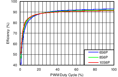
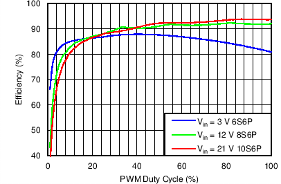
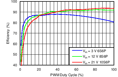
| Efficiency vs PWM Duty in PWM Mode | VIN = 12 V, VOUT = 6S6P, 8S6P, 10S6P, ICS = 20 mA, L = 10 µH | Figure 1 |
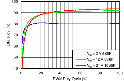
| Efficiency vs PWM Duty in PWM Mode | VIN = 3 V, 12 V, 21 V, VOUT = 6S6P, 8S6P, 10S6P, L = 10 µH | Figure 2 |
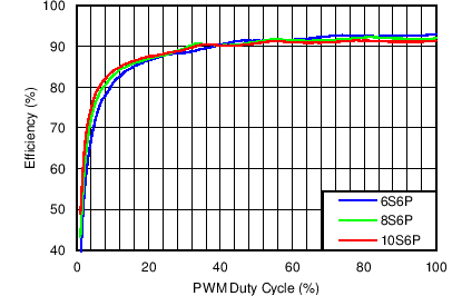
| Efficiency vs PWM duty in Mixed Mode | VIN = 12 V, VOUT = 6S6P, 8S6P, 10S6P, ICS = 20 mA, L = 10 µH | Figure 3 |
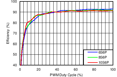
| Efficiency vs PWM duty in Mixed Mode | VIN = 3 V, 12 V, 21 V, VOUT = 6S6P, 8S6P, 10S6P, L = 10 µH | Figure 4 |
| Efficiency vs PWM duty in Analog Mode | VIN = 12 V, VOUT = 6S6P, 8S6P, 10S6P, ICS = 20 mA, L = 10 µH | Figure 5 |
| Efficiency vs PWM duty in Analog Mode | VIN = 3 V, 12 V, 21 V, VOUT = 6S6P, 8S6P, 10S6P, L = 10 µH | Figure 6 |
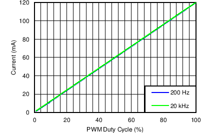
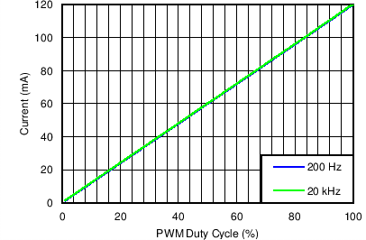
| Dimming Linearity in PWM Mode | VIN = 12 V, VOUT = 10S6P , FDIM = 200 Hz and 20 kHz, L = 10 µH | Figure 7 |
| Dimming Linearity in Mixed Mode | VIN = 12 V, VOUT = 10S6P , FDIM = 200 Hz and 20 kHz, L = 10 µH | Figure 8 |
| Dimming linearity in Analog Mode | VIN = 12 V, VOUT = 10S6P , FDIM = 200 Hz and 20 kHz, L = 10 µH | Figure 9 |
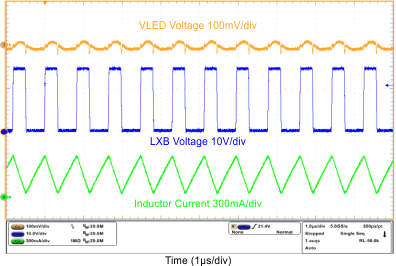
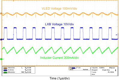
| Switch Waveform | VIN = 3 V, VOUT = 6S6P, Duty = 100%, L = 10 µH | Figure 10 |
| Switch Waveform | VIN = 12 V, VOUT = 10S6P, Duty = 100%, L = 10 µH | Figure 11 |
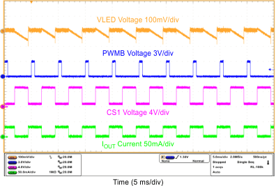
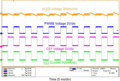
| Mixed-Mode Dimming Ripple | VIN = 12 V, VOUT = 10S6P, FDIM = 200 Hz, Duty = 50%, L = 10 µH | Figure 12 |
| Mixed-Mode Dimming Ripple | VIN = 12 V, VOUT = 10S6P, FDIM = 200 Hz, Duty = 12.5%, L = 10 µH | Figure 13 |
| Mixed-Mode Dimming Ripple | VIN = 12 V, VOUT = 10S6P, FDIM = 20 kHz, Duty = 12.5%, L = 10 µH | Figure 14 |
| PWM-Mode Dimming Ripple | VIN = 12 V, VOUT = 10S6P, FDIM = 200 Hz, Duty = 50%, L = 10 µH | Figure 15 |
| PWM-Mode Dimming Ripple | VIN = 12 V, VOUT = 10S6P, FDIM = 20 kHz, Duty = 50%, L = 10 µH | Figure 16 |
| FDIM = 200 Hz | Duty = 12.5% | |
| FDIM = 200 Hz | Duty = 50% | |

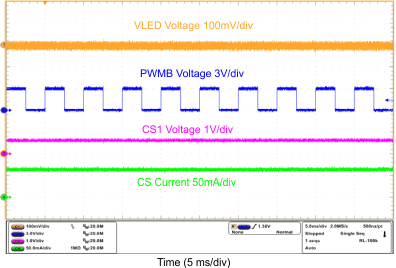
| FDIM = 200 Hz | Duty = 50% | |
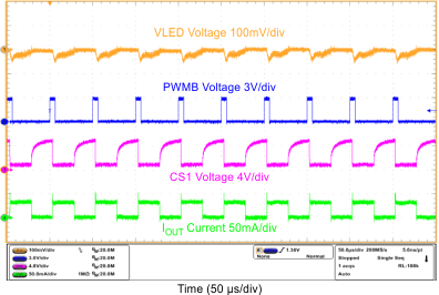
| FDIM = 20 kHz | Duty = 12.5% | |
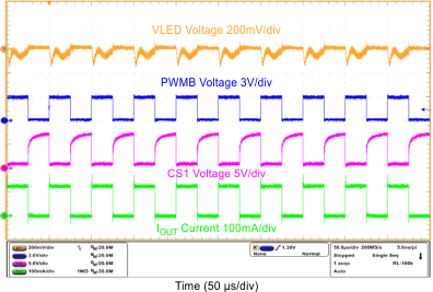
| FDIM = 20 kHz | Duty = 50% | |