SLVSA85E June 2010 – December 2016 TPS61187
PRODUCTION DATA.
- 1 Features
- 2 Applications
- 3 Description
- 4 Revision History
- 5 Pin Configuration and Functions
- 6 Specifications
-
7 Detailed Description
- 7.1 Overview
- 7.2 Functional Block Diagram
- 7.3 Feature Description
- 7.4
Device Functional Modes
- 7.4.1 Brightness Dimming Control
- 7.4.2 Adjustable PWM Dimming Frequency and Mode Selection (R_FPWM/MODE)
- 7.4.3 Mode Selection - Phase-Shift PWM Or Direct PWM Dimming
- 7.4.4 Overvoltage Clamp and Voltage Feedback (OVC / FB)
- 7.4.5 Current-Sink Open Protection
- 7.4.6 Overcurrent and Short-Circuit Protection
- 7.4.7 Thermal Protection
- 8 Application and Implementation
- 9 Power Supply Recommendations
- 10Layout
- 11Device and Documentation Support
- 12Mechanical, Packaging, and Orderable Information
Package Options
Mechanical Data (Package|Pins)
- RTJ|20
Thermal pad, mechanical data (Package|Pins)
- RTJ|20
Orderable Information
10 Layout
10.1 Layout Guidelines
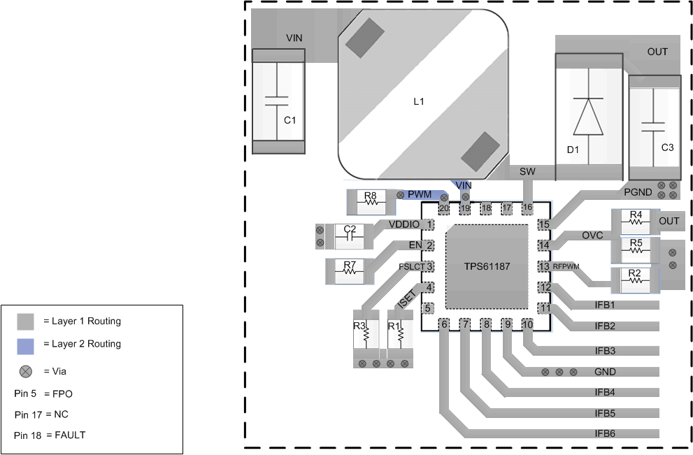
As for all switching power supplies, especially those providing high current and using high switching frequencies, layout is an important design step. If layout is not carefully done, the regulator could show instability as well as EMI problems. Therefore, use wide and short traces for high current paths. The input capacitor, C1 in Typical Application – Phase Shift PWM Mode, must not only be close to the VIN pin, but also to the GND pin in order to reduce the input ripple seen by the device. The input capacitor, C1 in Typical Application – Phase Shift PWM Mode, must also be placed close to the inductor. C2 is the filter and noise decoupling capacitor for the internal linear regulator powering the internal digital circuits; place C2 as close as possible between the VDDIO and AGND pins to prevent any noise insertion to the digital circuits. The SW pin carries high current with fast rising and falling edges. Therefore, the connection from the pin to the inductor and Schottky diode must be kept as short and wide as possible. It is also beneficial to have the ground of the output capacitor C3 close to the PGND pin because there is a large ground return current flowing between them. When laying out signal grounds, TI recommends using short traces separated from power ground traces and connecting them together at a single point, for example on the thermal pad. The thermal pad must be soldered on to the PCB and connected to the GND pin of the device. An additional thermal via can significantly improve power dissipation of the device.
10.2 Layout Example
 Figure 21. TPS61187 Layout Example