SNVSAF4C October 2015 – February 2021 TPS61193
PRODUCTION DATA
- 1 Features
- 2 Applications
- 3 Description
- 4 Revision History
- 5 Pin Configuration and Functions
-
6 Specifications
- 6.1 Absolute Maximum Ratings
- 6.2 ESD Ratings
- 6.3 Recommended Operating Conditions
- 6.4 Thermal Information
- 6.5 Electrical Characteristics (1) (1)
- 6.6 Internal LDO Electrical Characteristics
- 6.7 Protection Electrical Characteristics
- 6.8 Current Sinks Electrical Characteristics
- 6.9 PWM Brightness Control Electrical Characteristics
- 6.10 Boost and SEPIC Converter Characteristics
- 6.11 Logic Interface Characteristics
- 6.12 Typical Characteristics
- 7 Detailed Description
- 8 Application and Implementation
- 9 Power Supply Recommendations
- 10Layout
- 11Device and Documentation Support
- 12Mechanical, Packaging, and Orderable Information
Package Options
Mechanical Data (Package|Pins)
- PWP|20
Thermal pad, mechanical data (Package|Pins)
- PWP|20
Orderable Information
3 Description
The TPS61193 is a high-efficiency, low-EMI, easy-to-use LED driver with flexibility to support a wide range of applications. It has three high-precision current sinks that can be combined for higher current capability.
The TPS61193 has an integrated DC-DC supporting both boost and SEPIC mode operation. The converter has adaptive output voltage control based on the LED current sink headroom voltages. This feature minimizes the power consumption by adjusting the voltage to lowest sufficient level in all conditions. For EMI control the DC-DC converter supports spread spectrum for switching frequency and an external synchronization with dedicated pin.
The TPS61193 has wide input voltage range from 4.5 V to 40 V for robust support of different types of applications. The TPS61193 integrates extensive fault detection features. The device supports PWM brightness dimming ratio of 10 000:1 for 100-Hz input PWM frequency.
| PART NUMBER | PACKAGE | BODY SIZE (NOM) |
|---|---|---|
| TPS61193 | HTSSOP (20) | 6.50 mm × 4.40 mm |
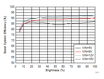
 System
Efficiency