SLVSEA0B january 2018 – june 2023 TPS61280D , TPS61280E , TPS61281D
PRODUCTION DATA
- 1
- 1 Features
- 2 Applications
- 3 Description
- 4 Revision History
- 5 Description (continued)
- 6 Device Comparison Table
- 7 Pin Configuration and Functions
- 8 Specifications
-
9 Detailed Description
- 9.1 Overview
- 9.2 Functional Block Diagram
- 9.3 Feature Description
- 9.4 Device Functional Modes
- 9.5 Programming
- 9.6
Register Maps
- 9.6.1 Slave Address Byte
- 9.6.2 Register Address Byte
- 9.6.3 I2C Registers, E2PROM, Write Protect
- 9.6.4 E2PROM Configuration Parameters
- 9.6.5 CONFIG Register [reset = 0x01]
- 9.6.6 VOUTFLOORSET Register [reset = 0x02]
- 9.6.7 VOUTROOFSET Register [reset = 0x03]
- 9.6.8 ILIMSET Register [reset = 0x04]
- 9.6.9 Status Register [reset = 0x05]
- 9.6.10 E2PROMCTRL Register [reset = 0xFF]
- 10Application and Implementation
- 11Power Supply Recommendations
- 12Layout
- 13Device and Documentation Support
- 14Mechanical, Packaging, and Orderable Information
Package Options
Mechanical Data (Package|Pins)
- YFF|16
Thermal pad, mechanical data (Package|Pins)
Orderable Information
10.2.1.2.2 Output Capacitor
For the output capacitor, it is recommended to use small ceramic capacitors placed as close as possible to the VOUT and GND pins of the IC. If, for any reason, the application requires the use of large capacitors which can not be placed close to the IC, using a smaller ceramic capacitor in parallel to the large one is highly recommended. This small capacitor should be placed as close as possible to the VOUT and GND pins of the IC. To get an estimate of the recommended minimum output capacitance, Equation 10 can be used.
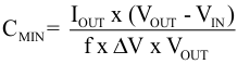
where
- f is the switching frequency which is 2.3 MHz (typ.) and ΔV is the maximum allowed output ripple.
With a chosen ripple voltage of 20 mV, a minimum effective capacitance of 10 μF is needed. The total ripple is larger due to the ESR and ESL of the output capacitor. This additional component of the ripple can be calculated using Equation 11
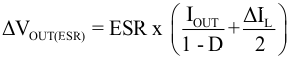
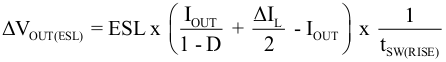
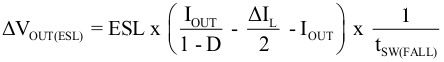
where
- IOUT = output current of the application
- D = duty cycle
- ΔIL = inductor ripple current
- tSW(RISE) = switch node rise time
- tSW(FALL) = switch node fall time
- ESR = equivalent series resistance of the used output capacitor
- ESL = equivalent series inductance of the used output capacitor
An MLCC capacitor with twice the value of the calculated minimum should be used due to DC bias effects. This is required to maintain control loop stability. The output capacitor requires either an X7R or X5R dielectric. Y5V and Z5U dielectric capacitors, aside from their wide variation in capacitance over temperature, become resistive at high frequencies. There are no additional requirements regarding minimum ESR. Larger capacitors cause lower output voltage ripple as well as lower output voltage drop during load transients.
In applications featuring high (pulsed) load currents (e.g. ≥ 2 Amps), it is recommended to run the converter with a reasonable amount of effective output capacitance and low-ESL device, for instance x2 22 µF X5R 6.3V (0603) MLCC capacitors connected in parallel with a 1 µF X5R 6.3 V (0306-2T) MLCC LL capacitor.
DC bias effect: high cap. ceramic capacitors exhibit DC bias effects, which have a strong influence on the device's effective capacitance. Therefore the right capacitor value has to be chosen very carefully. Package size and voltage rating in combination with material are responsible for differences between the rated capacitor value and it's effective capacitance. For instance, a 10 µF X5R 6.3 V (0603) MLCC capacitor would typically show an effective capacitance of less than 5 µF (under 3.5 V bias condition, high temperature).
For RF Power Amplifier applications, the output capacitor loading is combined between the dc/dc converter and the RF Power Amplifier (x2 10 µF X5R 6.3 V (0603) + PA input cap 4.7 µF X5R 6.3 V (0402)) are recommended.
High values of output capacitance are mainly achieved by putting capacitors in parallel. This reduces the overall series resistance (ESR) to very low values. This results in almost no voltage ripple at the output and therefore the regulation circuit has no voltage drop to react on. Nevertheless, for accurate output voltage regulation even with low ESR, the regulation loop can switch to a pure comparator regulation scheme.