SLVSEA0B january   2018  – june 2023 TPS61280D , TPS61280E , TPS61281D

PRODUCTION DATA  

  1.   1
  2. Features
  3. Applications
  4. Description
  5. Revision History
  6. Description (continued)
  7. Device Comparison Table
  8. Pin Configuration and Functions
  9. Specifications
    1. 8.1 Absolute Maximum Ratings
    2. 8.2 ESD Ratings
    3. 8.3 Recommended Operating Conditions
    4. 8.4 Thermal Information
    5. 8.5 Electrical Characteristics
    6. 8.6 I2C Interface Timing Characteristics #GUID-BD85FD7C-B9AF-4F5D-9DFF-CD61365A592A/SLVS5401494
    7. 8.7 I2C Timing Diagrams
    8. 8.8 Typical Characteristics
  10. Detailed Description
    1. 9.1 Overview
    2. 9.2 Functional Block Diagram
    3. 9.3 Feature Description
      1. 9.3.1 Voltage Scaling Management (VSEL)
      2. 9.3.2 Spread Spectrum, PWM Frequency Dithering
    4. 9.4 Device Functional Modes
      1. 9.4.1 Power-Save Mode
      2. 9.4.2 Pass-Through Mode
      3. 9.4.3 Mode Selection
      4. 9.4.4 Current Limit Operation
      5. 9.4.5 Start-Up and Shutdown Mode
      6. 9.4.6 Undervoltage Lockout
      7. 9.4.7 Thermal Shutdown
      8. 9.4.8 Fault State and Power-Good
    5. 9.5 Programming
      1. 9.5.1 Serial Interface Description (TPS61280D/E)
      2. 9.5.2 Standard-, Fast-, Fast-Mode Plus Protocol
      3. 9.5.3 HS-Mode Protocol
      4. 9.5.4 TPS6128xD/E I2C Update Sequence
    6. 9.6 Register Maps
      1. 9.6.1  Slave Address Byte
      2. 9.6.2  Register Address Byte
      3. 9.6.3  I2C Registers, E2PROM, Write Protect
      4. 9.6.4  E2PROM Configuration Parameters
      5. 9.6.5  CONFIG Register [reset = 0x01]
      6. 9.6.6  VOUTFLOORSET Register [reset = 0x02]
      7. 9.6.7  VOUTROOFSET Register [reset = 0x03]
      8. 9.6.8  ILIMSET Register [reset = 0x04]
      9. 9.6.9  Status Register [reset = 0x05]
      10. 9.6.10 E2PROMCTRL Register [reset = 0xFF]
  11. 10Application and Implementation
    1. 10.1 Application Information
    2. 10.2 Typical Application
      1. 10.2.1 TPS61281D with 2.5V-4.35 VIN, 1500 mA Output Current (TPS61280D with default I2C Configuration)
        1. 10.2.1.1 Design Requirement
        2. 10.2.1.2 Detailed Design Parameters
          1. 10.2.1.2.1 Inductor Selection
          2. 10.2.1.2.2 Output Capacitor
          3. 10.2.1.2.3 Input Capacitor
          4. 10.2.1.2.4 Checking Loop Stability
        3. 10.2.1.3 Application Performance Curves
      2. 10.2.2 TPS61282D with 2.5V-4.35 VIN, 2000 mA Output Current (TPS61280D with I2C Programmable)
        1. 10.2.2.1 Design Requirements
        2. 10.2.2.2 Detailed Design Procedures
        3. 10.2.2.3 Application Performance Curves
  12. 11Power Supply Recommendations
  13. 12Layout
    1. 12.1 Layout Guidelines
    2. 12.2 Layout Example
    3. 12.3 Thermal Information
  14. 13Device and Documentation Support
    1. 13.1 Device Support
      1. 13.1.1 Third-Party Products Disclaimer
    2. 13.2 Receiving Notification of Documentation Updates
    3. 13.3 Support Resources
    4. 13.4 Trademarks
    5. 13.5 Electrostatic Discharge Caution
    6. 13.6 Glossary
  15. 14Mechanical, Packaging, and Orderable Information
    1. 14.1 Package Summary

Package Options

Mechanical Data (Package|Pins)
Thermal pad, mechanical data (Package|Pins)
Orderable Information

Description

The TPS6128xD/E device provides a power supply solution for products powered by either by a Li-Ion, Nickel-Rich, Silicon Anode, Li-Ion or LiFePO4 battery. The voltage range is optimized for single-cell portable applications like in smart-phones or tablet PCs.

Used as a high-power pre-regulator, the TPS6128xD/E extends the battery run-time and overcomes input current- and voltage limitations of the powered system.

While in shutdown, the TPS6128xD/E operates in a true pass-through mode with only 3-µA quiescent consumption for longest battery shelf life.

During operation, when the battery is at a good state-of-charge, a low-ohmic, high-efficient integrated pass-through path connects the battery to the powered system.

If the battery gets to a lower state of charge and its voltage becomes lower than the desired minimum system voltage, the device seamlessly transits into boost mode to uses the full battery capacity.

Device Information(1)
PART NUMBERPACKAGEBODY SIZE (NOM)
TPS61280DDSBGA (16)1.66 mm x 1.66 mm
TPS61281D
TPS61282D
TPS61280E
For all available packages, see the orderable addendum at the end of the datasheet.
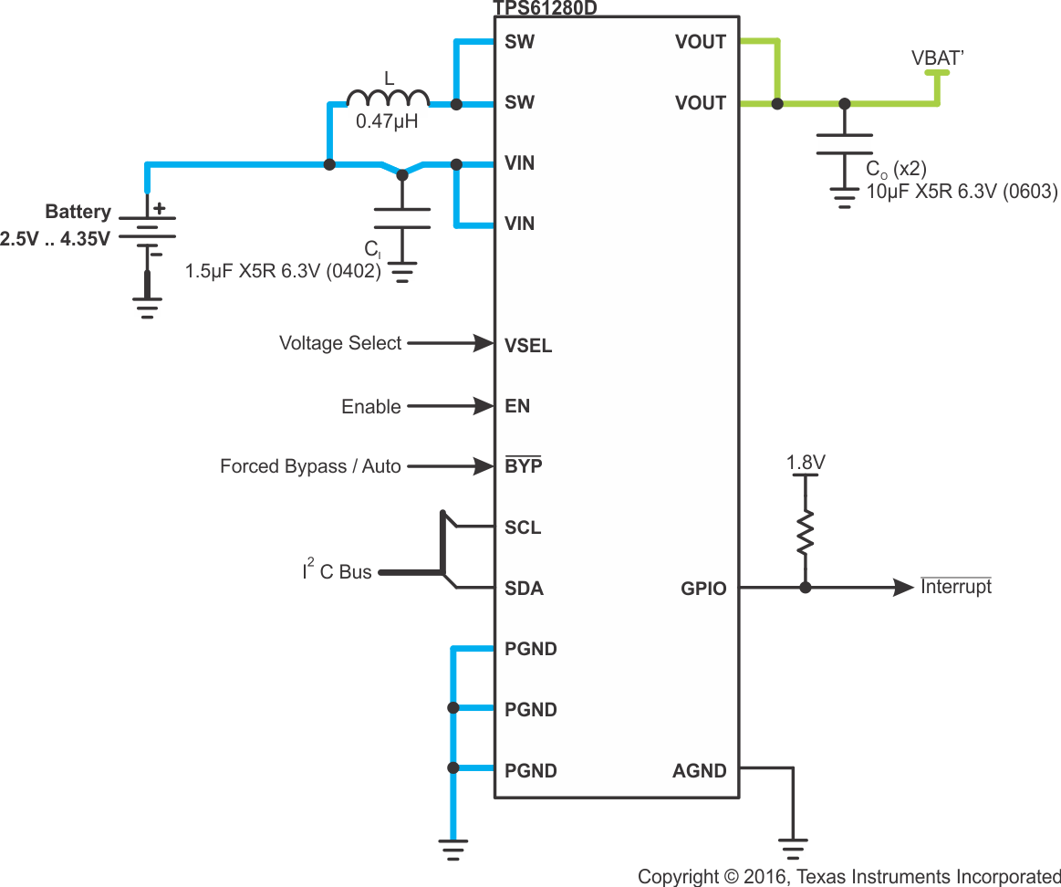
GUID-BCCF4A88-434E-45F7-8B00-E61B1ABAE5D9-low.gif Simplified Schematic