SLVSAA2D March 2010 – January 2016 TPS65182 , TPS65182B
PRODUCTION DATA.
- 1 Features
- 2 Applications
- 3 Description
- 4 Revision History
- 5 Pin Configuration and Functions
- 6 Specifications
-
7 Detailed Description
- 7.1 Overview
- 7.2 Functional Block Diagram
- 7.3
Feature Description
- 7.3.1 Modes of Operation
- 7.3.2 Mode Transistions
- 7.3.3 Wake-Up and Power Up Sequencing
- 7.3.4 Dependencies Between Rails
- 7.3.5 Soft-Start
- 7.3.6 VCOM Adjustment
- 7.3.7 VPOS and VNEG Supply Tracking
- 7.3.8 Fault Handling and Recovery
- 7.3.9 Power Good Pin
- 7.3.10 Panel Temperature Monitoring
- 7.3.11 NTC Bias Circuit
- 7.4 Device Functional Modes
- 7.5 Register Maps
- 8 Application and Implementation
- 9 Power Supply Recommendations
- 10Layout
- 11Device and Documentation Support
- 12Mechanical, Packaging, and Orderable Information
Package Options
Mechanical Data (Package|Pins)
- RGZ|48
Thermal pad, mechanical data (Package|Pins)
- RGZ|48
Orderable Information
8 Application and Implementation
NOTE
Information in the following applications sections is not part of the TI component specification, and TI does not warrant its accuracy or completeness. TI’s customers are responsible for determining suitability of components for their purposes. Customers should validate and test their design implementation to confirm system functionality.
8.1 Application Information
The TPS65185 device is used to power display screens in E-book applications, specifically E-Ink Vizplex display, by connecting the screen to the positive and negative charge pump, LDOs 1 and 2, and VCOM rails. The display screens size that can be supported up to 9.7 inches.
8.2 Typical Application
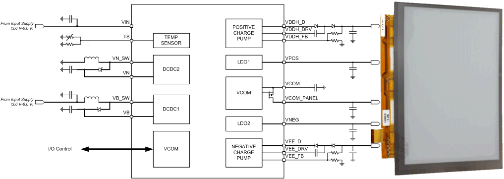 Figure 9. Typical Application Schematic
8.2.1 Design Requirements
For this design example, use the parameters listed in Table 3 as the input parameters.
Table 3. Design Parameters
| VOLTAGE | SEQUENCE (STROBE) | |
|---|---|---|
| VNEG (LDO2) | –15 V | 1 |
| VEE (Charge pump 2) | –20 V | 2 |
| VPOS (LDO1) | 15 V | 3 |
| VDDH (Charge pump 1) | 22 V | 4 |
8.2.2 Detailed Design Procedure
For the positive boost regulator (DCDC1) a 10-µF capacitor can be used as the input capacitor value; two 4.7-µF capacitor are used as output capacitors to reduce ESR along with a 2.2-µH inductor. For the inverting buck-boost regulator (DCDC2), an 10-µF capacitor can be used at the input capacitor value; A 10-µF and 4.7-µF capacitor are used as output capacitors to reduce ESR, with a 4.7-µH inductor. Capacitor ESR for all capacitors should be around 20 mΩ, and ceramic X5R material. These are the typical the values used, additional inductor and capacitor values can be used for improved functionality, but the parts should be rated the same as the recommended external components listed in Table 4.
Table 4. Recommended External Components
| PART NUMBER | VALUE | SIZE | MANUFACTURER |
|---|---|---|---|
| INDUCTORS | |||
| LQH44PN4R7MP0 | 4.7 µH | 4 mm × 4 mm × 1.65 mm | Murata |
| NR4018T4R7M | 4.7 µH | 4 mm × 4 mm × 1.8 mm | Taiyo Yuden |
| VLS252015ET-2R2M | 2.2 µH | 2 mm × 2.5 mm × 1.5 mm | TDK |
| NR4012T2R2M | 2.2 µH | 4 mm × 4 mm × 1.2 mm | Taiyo Yuden |
| CAPACITORS | |||
| GRM21BC81E475KA12L | 4.7 µF, 25 V, X6S | 805 | Murata |
| GRM32ER71H475KA88L | 4.7 µF, 50 V, X7R | 1210 | Murata |
| All other capacitors | X5R or better | — | — |
| DIODES | |||
| BAS3010 | — | SOD-323 | Infineon |
| MBR130T1 | — | SOD-123 | ON-Semi |
| BAV99 | — | SOT-23 | Fairchild |
| THERMISTOR | |||
| NCP18XH103F03RB | 10 kΩ | 603 | Murata |
8.2.3 Application Curves
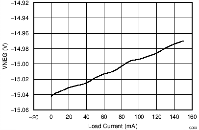 Figure 10. Load Current vs VNEG
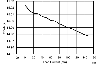 Figure 12. Load Current vs VPOS
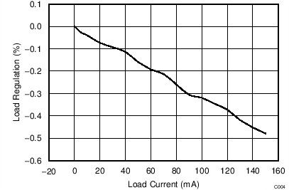 Figure 11. Load Current vs Load Regulation
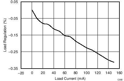 Figure 13. Load Current vs Load Regulation