SLVSAQ8G February 2011 – September 2017 TPS65185
PRODUCTION DATA.
- 1 Features
- 2 Applications
- 3 Description
- 4 Revision History
- 5 Description (continued)
- 6 Pin Configuration and Functions
- 7 Specifications
-
8 Detailed Description
- 8.1 Overview
- 8.2 Functional Block Diagram
- 8.3
Feature Description
- 8.3.1 Wake-Up and Power-Up Sequencing
- 8.3.2 Dependencies Between Rails
- 8.3.3 Soft Start
- 8.3.4 Active Discharge
- 8.3.5 VPOS/VNEG Supply Tracking
- 8.3.6 V3P3 Power Switch
- 8.3.7 VCOM Adjustment
- 8.3.8 Fault Handling And Recovery
- 8.3.9 Power Good Pin
- 8.3.10 Interrupt Pin
- 8.3.11 Panel Temperature Monitoring
- 8.4 Device Functional Modes
- 8.5 Programming
- 8.6
Register Maps
- 8.6.1 Thermistor Readout (TMST_VALUE) Register (address = 0x00h) [reset = N/A]
- 8.6.2 Enable (ENABLE) Register (address = 0x01h) [reset = 0h]
- 8.6.3 Voltage Adjustment (VADJ) Register (address = 0x02h) [reset = 23h]
- 8.6.4 VCOM 1 (VCOM1) Register (address = 0x03h) [reset = 7Dh]
- 8.6.5 VCOM 2 (VCOM2) Register (address = 0x04h) [reset = 04h]
- 8.6.6 Interrupt Enable 1 (INT_EN1) Register (address = 0x05h) [reset = 7Fh]
- 8.6.7 Interrupt Enable 2 (INT_EN2) Register (address = 0x06h) [reset = FFh]
- 8.6.8 Interrupt 1 (INT1) Register (address = 0x07h) [reset = 0h]
- 8.6.9 Interrupt 2 (INT2) Register (address = 0x08h) [reset = N/A]
- 8.6.10 Power-Up Sequence 0 (UPSEQ0) Register (address = 0x09h) [reset = E4h]
- 8.6.11 Power-Up Sequence 1 (UPSEQ1) Register (address = 0x0Ah) [reset = 55h]
- 8.6.12 Power-Down Sequence 0 (DWNSEQ0) Register (address = 0x0Bh) [reset = 1Eh]
- 8.6.13 Power-Down Sequence 1 (DWNSEQ1) Register (address = 0x0Ch) [reset = E0h]
- 8.6.14 Thermistor 1 (TMST1) Register (address = 0x0Dh) [reset = 20h]
- 8.6.15 Thermistor 2 (TMST2) Register (address = 0x0Eh) [reset = 78h]
- 8.6.16 Power Good Status (PG) Register (address = 0x0Fh) [reset = 0h]
- 8.6.17 Revision and Version Control (REVID) Register (address = 0x10h) [reset = 45h]
- 9 Application and Implementation
- 10Power Supply Recommendations
- 11Layout
- 12Device and Documentation Support
- 13Mechanical, Packaging, and Orderable Information
Package Options
Mechanical Data (Package|Pins)
Thermal pad, mechanical data (Package|Pins)
Orderable Information
9 Application and Implementation
NOTE
Information in the following applications sections is not part of the TI component specification, and TI does not warrant its accuracy or completeness. TI’s customers are responsible for determining suitability of components for their purposes. Customers should validate and test their design implementation to confirm system functionality.
9.1 Application Information
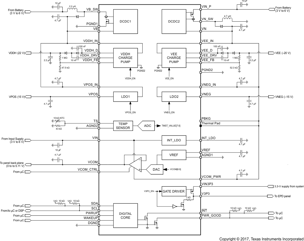
The TPS65185x device is used to power display screens in E-book applications, specifically E-Ink Vizplex display, by connecting the screen to the positive and negative charge pump, LDO1, LDO2, and VCOM rails. The device supports display screens up to 9.7 inches.
9.2 Typical Application
9.2.1 Design Requirements
For this design example, use the parameters listed in Table 20 as the input parameters.
Table 20. Design Parameters
| VOLTAGE | SEQUENCE (STROBE) | |
|---|---|---|
| VNEG (LDO2) | –15 V | 1 |
| VEE (Charge pump 2) | –20 V | 2 |
| VPOS (LDO1) | 15 V | 3 |
| VDDH (Charge pump 1) | 22 V | 4 |
9.2.2 Detailed Design Procedure
For the positive boost regulator (DCDC1) a 10-μF capacitor can be used as the input capacitor value; two 4.7-μF capacitors are used as output capacitors to reduce ESR along with a 2.2-μH inductor. For the inverting buck-boost regulator (DCDC2), a 10-μF capacitor can be used at the input capacitor value; two 4.7-μF capacitors are used as output capacitors to reduce ESR along with a 4.7-μH inductor. The charge pump pins VDDH_D and VEE_D require 100-nF capacitors to ground for reliable operation. An ESR capacitor with a value of 20 mΩ is expected for all capacitors, and ceramic X5R material or better is recommended. These values are the typical the values used; additional inductor and capacitor values can be used for improved functionality; however, the components should be rated the same as the recommended external components listed in Table 21.
Table 21. Recommended External Components
| PART NUMBER | VALUE | SIZE | MANUFACTURER |
|---|---|---|---|
| INDUCTORS | |||
| LQH44PN4R7MP0 | 4.7 µH | 4 mm × 4 mm × 1.65 mm | Murata |
| NR4018T4R7M | 4.7 µH | 4 mm × 4 mm × 1.8 mm | Taiyo Yuden |
| VLS252015ET-2R2M | 2.2 µH | 2 mm × 2.5 mm × 1.5 mm | TDK |
| NR4012T2R2M | 2.2 µH | 4 mm × 4 mm × 1.2 mm | Taiyo Yuden |
| CAPACITORS | |||
| GRM21BC81E475KA12L | 4.7 µF, 25 V, X6S | 805 | Murata |
| GRM32ER71H475KA88L | 4.7 µF, 50 V, X7R | 1210 | Murata |
| All other capacitors | X5R or better | — | — |
| DIODES | |||
| BAS3010 | — | SOD-323 | Infineon |
| MBR130T1 | — | SOD-123 | ON-Semi |
| BAV99 | — | SOT-23 | Fairchild |
| THERMISTOR | |||
| NCP18XH103F03RB | 10 kΩ | 603 | Murata |
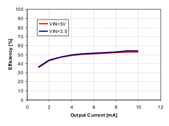
9.2.3 Application Curves
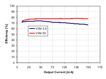
| T = 25°C |
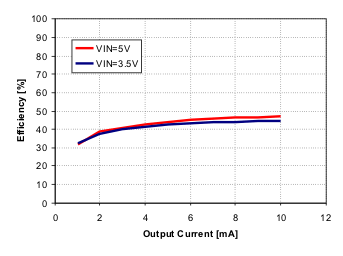
| T = 25°C |
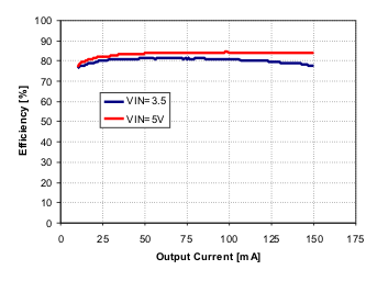
| T = 25°C |
| T = 25°C |
