SLVSD66 September 2015 TPS65233-1
PRODUCTION DATA.
- 1 Features
- 2 Applications
- 3 Description
- 4 Revision History
- 5 Pin Configuration and Functions
- 6 Specifications
- 7 Detailed Description
- 8 Application and Implementation
- 9 Power Supply Recommendations
- 10Layout
- 11Device and Documentation Support
- 12Mechanical, Packaging, and Orderable Information
Package Options
Mechanical Data (Package|Pins)
- RTE|16
Thermal pad, mechanical data (Package|Pins)
- RTE|16
Orderable Information
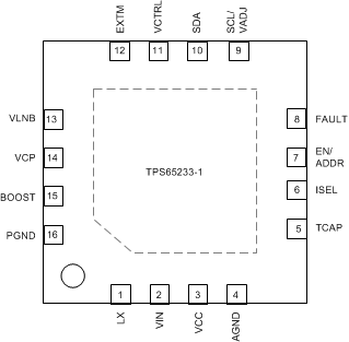
5 Pin Configuration and Functions
RTE Package
12-Pin WQFN
Top View

Exposed pad must be soldered to PCB for optimal thermal performance.
Pin Functions
| PIN | DESCRIPTION | |
|---|---|---|
| NAME | NUMBER | |
| AGND | 4 | Analog ground. Connect all ground pins and power pad together. |
| BOOST | 15 | Output of the boost regulator and input voltage of the internal linear regulator |
| EN/ADDR | 7 | Enable pin to enable the whole chip; pull to ground to disable output, output will be pulled to ground. For I2C interface, pulling this pin high or low gives different I2C addresses. |
| EXTM | 12 | External modulation logic input pin which activates the 22-kHz tone output, feeding signal can be 22-kHz tone or logic high or low. |
| FAULT | 8 | This pin is an open drain output pin, it goes low if any fault flag is set. |
| ISEL | 6 | Connect a resistor to this pin to set the LNB output current limit. |
| LX | 1 | Switching node of the boost converter |
| PGND | 16 | Power ground for boost converter |
| SCL/VADJ | 9 | I2C compatible clock input; if I2C function is not used, connect this pin to low set output voltage 13 V/18 V, connect to high set output voltage 13.4 V/18.6 V |
| SDA | 10 | I2C compatible bi-directional data |
| TCAP | 5 | Connect a capacitor to this pin to set the rise time and fall time of the LNB output between 13 V and 18 V. |
| VCC | 3 | Internal 6.5-V power supply bias. Connect a 1-µF ceramic capacitor from this pin to ground. When VIN is 5 V, connect VCC to VIN. |
| VCP | 14 | Gate drive supply voltage, output of charge pump, connect a capacitor between this pin to pin BOOST. |
| VCTRL | 11 | Logic control pin for 13-V or 18-V voltage selection at LNB output |
| VIN | 2 | Input of internal linear regulator |
| VLNB | 13 | Output of the LNB power supply connected to satellite receiver or switch |
| Thermal pad | — | Must be soldered to PCB for optimal thermal performance. Have thermal vias on the PCB to enhance power dissipation. |