SLVSCS9D december 2014 – may 2023 TPS65263-Q1
PRODUCTION DATA
- 1
- 1 Features
- 2 Applications
- 3 Description
- 4 Revision History
- 5 Pin Configuration and Functions
- 6 Specifications
-
7 Detailed Description
- 7.1 Overview
- 7.2 Functional Block Diagram
- 7.3
Feature Description
- 7.3.1 Adjusting the Output Voltage
- 7.3.2 Enable and Adjusting UVLO
- 7.3.3 Soft-Start Time
- 7.3.4 Power-Up Sequencing
- 7.3.5 V7V Low-Dropout Regulator and Bootstrap
- 7.3.6 Out-of-Phase Operation
- 7.3.7 Output Overvoltage Protection (OVP)
- 7.3.8 PSM
- 7.3.9 Slope Compensation
- 7.3.10 Overcurrent Protection
- 7.3.11 Power Good
- 7.3.12 Thermal Shutdown
- 7.4 Device Functional Modes
- 7.5 Register Maps
- 8 Application and Implementation
- 9 Device and Documentation Support
- 10Mechanical, Packaging, and Orderable Information
Package Options
Mechanical Data (Package|Pins)
- RHB|32
Thermal pad, mechanical data (Package|Pins)
- RHB|32
Orderable Information
7.3.3 Soft-Start Time
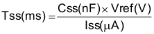
The voltage on the respective SS pin controls the start-up of buck output. When the voltage on the SS pin is less than the internal 0.6-V reference, The TPS65263-Q1 regulates the internal feedback voltage to the voltage on the SS pin instead of 0.6 V. The SS pin can be used to program an external soft-start function or to allow output of buck to track another supply during start-up. The device has an internal pullup current source of 5.2 µA (typical) that charges an external soft-start capacitor to provide a linear ramping voltage at the SS pin. The TPS65263-Q1 regulates the internal feedback voltage to the voltage on the SS pin, allowing VOUT to rise smoothly from 0 V to its regulated voltage without inrush current. The soft-start time can be calculated approximately by Equation 4.
Many of the common power-supply sequencing methods can be implemented using the SSx and ENx pins. Figure 7-6 shows the method implementing ratiometric sequencing by connecting the SSx pins of three buck channels together. The regulator outputs ramp up and reach regulation at the same time. When calculating the soft-start time, the pullup current source must be tripled in Equation 4.
 Figure 7-6 Ratiometric Power-Up Using SSx Pins
The user can implement simultaneous power-supply sequencing by connecting the capacitor to the SSx pin, shown in Figure 7-7. Using Equation 4 and Equation 5, the capacitors can be calculated.
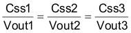
 Figure 7-7 Simultaneous Start-up Sequence Using SSx Pins