SLVSDA6 October 2016 TPS65266-1
PRODUCTION DATA.
- 1 Features
- 2 Applications
- 3 Description
- 4 Revision History
- 5 Pin Configuration and Functions
- 6 Specifications
-
7 Detailed Description
- 7.1 Overview
- 7.2 Functional Block Diagram
- 7.3
Feature Description
- 7.3.1 Adjusting the Output Voltage
- 7.3.2 Enable and Adjusting UVLO
- 7.3.3 Soft-Start Time
- 7.3.4 Power-Up Sequencing
- 7.3.5 Bootstrap Voltage and BST-LX UVLO
- 7.3.6 Out of Phase Operation
- 7.3.7 Output Overvoltage Protection (OVP)
- 7.3.8 Slope Compensation
- 7.3.9 Overcurrent Protection
- 7.3.10 Power Good
- 7.3.11 Adjustable Switching Frequency
- 7.3.12 PSM
- 7.3.13 Thermal Shutdown
- 7.4 Device Functional Modes
- 8 Application and Implementation
- 9 Power Supply Recommendations
- 10Layout
- 11Device and Documentation Support
- 12Mechanical, Packaging, and Orderable Information
Package Options
Mechanical Data (Package|Pins)
- RHB|32
Thermal pad, mechanical data (Package|Pins)
- RHB|32
Orderable Information
8 Application and Implementation
NOTE
Information in the following applications sections is not part of the TI component specification, and TI does not warrant its accuracy or completeness. TI’s customers are responsible for determining suitability of components for their purposes. Customers should validate and test their design implementation to confirm system functionality.
8.1 Application Information
The device is a triple-synchronous step-down DC/DC converter. It is typically used to convert a higher DC voltage to lower DC voltages with a continuously available output current of 3 A/2 A/2 A. The following design procedure can be used to select component values for the TPS65266-1. This section presents a simplified discussion of the design process.
8.2 Typical Application
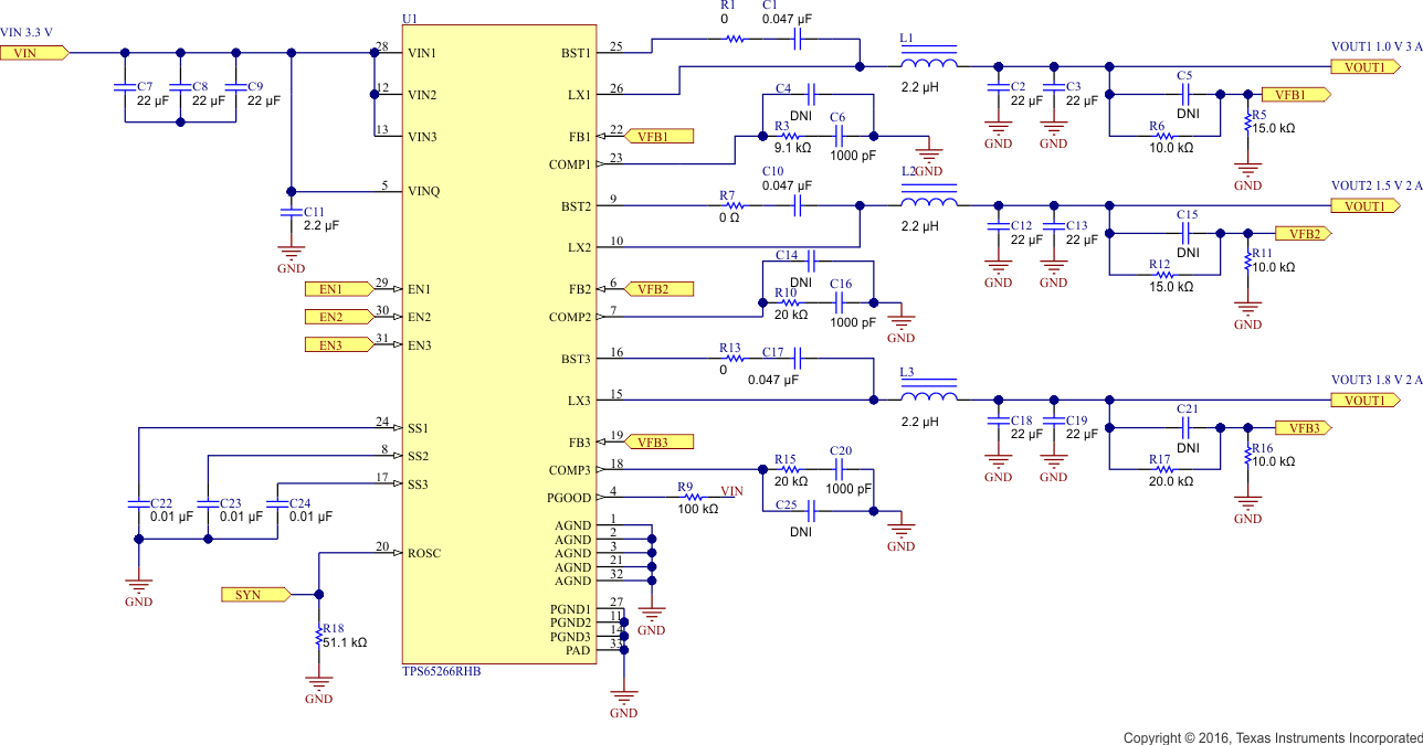 Figure 33. Typical Application Schematic
8.2.1 Design Requirements
This example details the design of a triple-synchronous step-down converter. The designer must know a few parameters to start the design process. These parameters are typically determined at the system level. For this example, start with the following known parameters in Table 2.
Table 2. Design Parameters
| Parameter | Value |
|---|---|
| Vout1 | 1.0 V |
| Iout1 | 3 A |
| Vout2 | 1.5 V |
| Iout2 | 2 A |
| Vout3 | 1.8 V |
| Iout3 | 2 A |
| Transient response 1-A load step | ±5% |
| Input voltage | 5.0 V normal, 2.7 to 6 V |
| Output voltage ripple | ±1% |
| Switching frequency | 1 MHz |
8.2.2 Detailed Design Procedure
8.2.2.1 Output Inductor Selection
To calculate the value of the output inductor, use Equation 8. LIR is a coefficient that represents the amount of inductor ripple current relative to the maximum output current. The inductor ripple current is filtered by the output capacitor. Therefore, choosing high inductor ripple currents impact the selection of the output capacitor because the output capacitor must have a ripple current rating equal to or greater than the inductor ripple current. In general, the inductor ripple value is at the discretion of the designer; however, LIR is normally from 0.1 to 0.3 for the majority of applications.

For the output filter inductor, it is important that the RMS current and saturation current ratings not be exceeded. The RMS and peak inductor current can be found from Equation 10 and Equation 11.


The current flowing through the inductor is the inductor ripple current plus the output current. During power-up, faults, or transient load conditions, the inductor current can increase above the calculated peak inductor current level calculated previously. In transient conditions, the inductor current can increase up to the switch current limit of the device. For this reason, the most conservative approach is to specify an inductor with a saturation current rating equal to or greater than the switch current limit rather than the peak inductor current.
8.2.2.2 Output Capacitor Selection
The three primary considerations for selecting the value of the output capacitor are: the output capacitor determines the modulator pole, the output voltage ripple, and how the regulator responds to a large change in load current. The output capacitance must be selected based on the most stringent of these three criteria.
The first criterion is the desired response to a large change in the load current. The output capacitor needs to supply the load with current when the regulator cannot. This situation would occur if there are desired hold-up times for the regulator where the output capacitor must hold the output voltage above a certain level for a specified amount of time after the input power is removed. The regulator is also temporarily not able to supply sufficient output current if there is a large, fast increase in the current needs of the load such as a transition from no load to full load. The regulator usually needs two or more clock cycles for the control loop to see the change in load current and output voltage and adjust the duty cycle to react to the change. The output capacitor must be sized to supply the extra current to the load until the control loop responds to the load change. The output capacitance must be large enough to supply the difference in current for two clock cycles while only allowing a tolerable amount of droop in the output voltage. Equation 12 shows the minimum output capacitance necessary to accomplish this.

where
- ΔIout is the change in output current.
- ƒSW is the regulator's switching frequency.
- ΔVout is the allowable change in the output voltage.
Equation 13 calculates the minimum output capacitance needed to meet the output voltage ripple specification.

where
- ƒSW is the switching frequency.
- Vripple is the maximum allowable output voltage ripple.
- Iripple is the inductor ripple current.
Equation 14 calculates the maximum ESR an output capacitor can have to meet the output voltage ripple specification.

Additional capacitance deratings for aging, temperature, and DC bias should be factored in, which increase this minimum value. Capacitors generally have limits to the amount of ripple current they can handle without failing or producing excess heat. An output capacitor that can support the inductor ripple current must be specified. Some capacitor data sheets specify the root mean square (RMS) value of the maximum ripple current. Equation 15 can be used to calculate the RMS ripple current the output capacitor needs to support.

8.2.2.3 Input Capacitor Selection
The TPS65266-1 requires a high-quality ceramic, type X5R or X7R, input decoupling capacitor of at least 10 μF of effective capacitance on the VIN input voltage pins. In some applications, additional bulk capacitance may also be required for the VIN input. The effective capacitance includes any DC bias effects. The voltage rating of the input capacitor must be greater than the maximum input voltage. The capacitor must also have a ripple current rating greater than the maximum input current ripple of the TPS65266-1. Calculate the input ripple current using Equation 16.

The value of a ceramic capacitor varies significantly over temperature and the amount of DC bias applied to the capacitor. The capacitance variations due to temperature can be minimized by selecting a dielectric material that is stable over temperature. X5R and X7R ceramic dielectrics are usually selected for power regulator capacitors because they have a high capacitance-to-volume ratio and are fairly stable over temperature. The output capacitor must also be selected with the DC bias taken into account. The capacitance value of a capacitor decreases as the DC bias across a capacitor increases. The input capacitance value determines the input ripple voltage of the regulator. Calculate the input voltage ripple using Equation 17.

8.2.2.4 Loop Compensation
The TPS65266-1 incorporates a peak current mode control scheme. The error amplifier is a transconductance amplifier with a gain of 290 µS. A typical type II compensation circuit adequately delivers a phase margin between 30° and 90°. Cb adds a high-frequency pole to attenuate high-frequency noise when needed. To calculate the external compensation components, follow these steps.
- Select switching frequency, ƒSW, that is appropriate for application depending on L and C sizes, output ripple, EMI, and so forth. Switching frequency between 500 kHz to 1.5 MHz gives best trade-off between performance and cost. To optimize efficiency, lower switching frequency is desired.
- Set up crossover frequency, ƒc, which is typically between 1 / 5 and 1 / 20 of ƒSW.
- RC can be determined by:
- Gm_EA is the error amplifier gain (290 µS).
- Gm_PS is the power stage voltage to current conversion gain (10 A/V).
- Calculate CC by placing a compensation zero at or before the dominant pole

- Optional Cb can be used to cancel the zero from the ESR associated with CO.
- Type III compensation can be implemented with the addition of one capacitor, C1. This allows for slightly higher loop bandwidths and higher phase margins. If used, C1 is calculated from Equation 21.

where


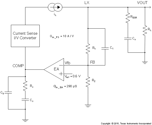 Figure 34. DC/DC Loop Compensation
8.2.3 Application Curves
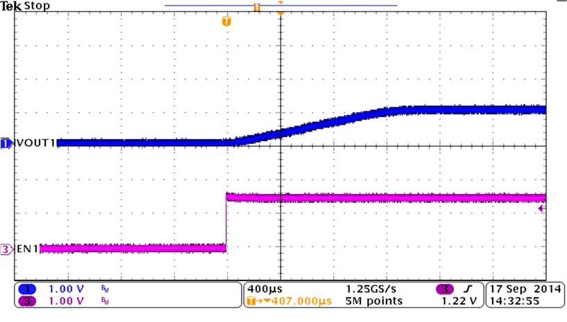
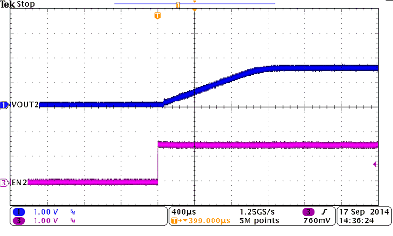

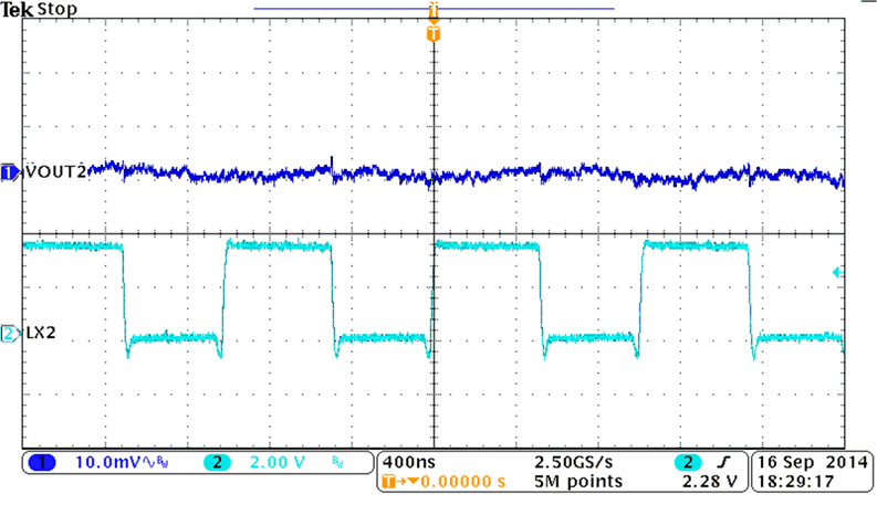
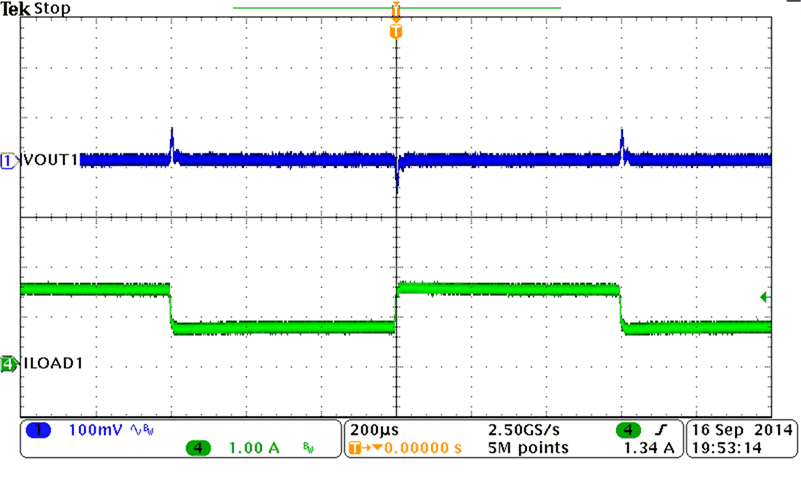
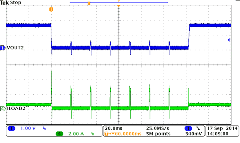
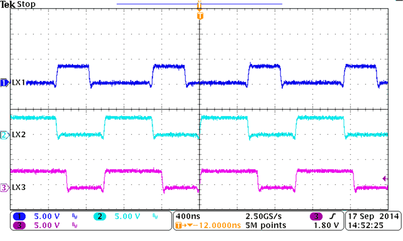
| SR = 0.25 A/µs | ||
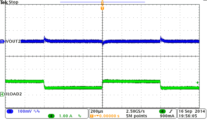
| SR = 0.25 A/µs | ||
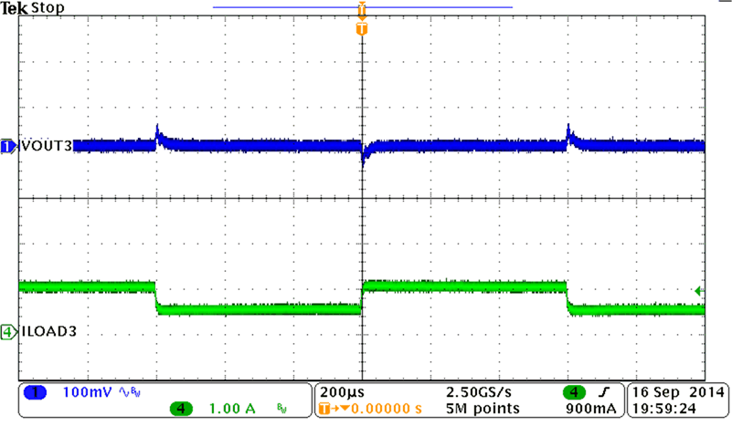
| SR = 0.25 A/µs | ||
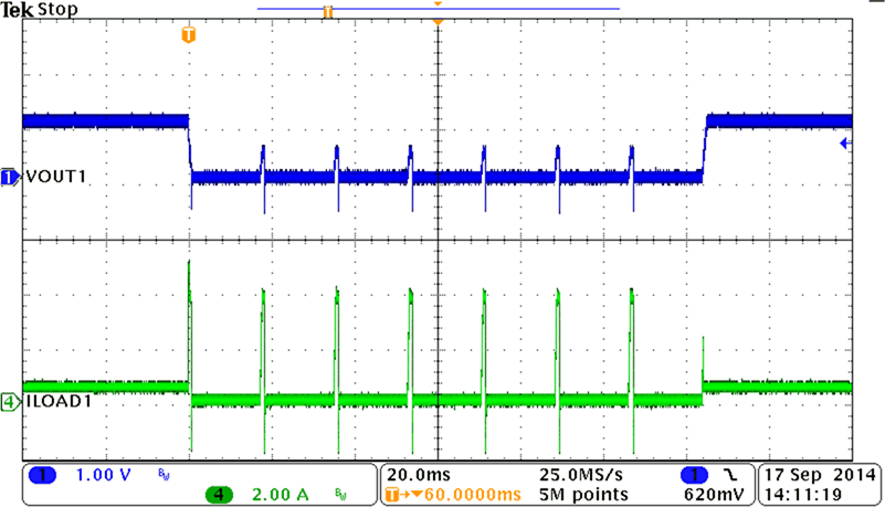
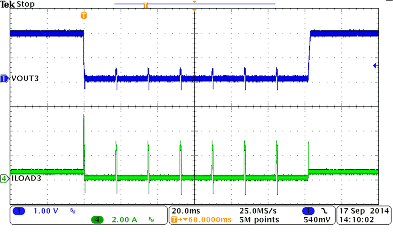
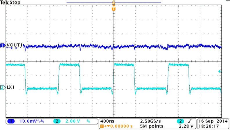
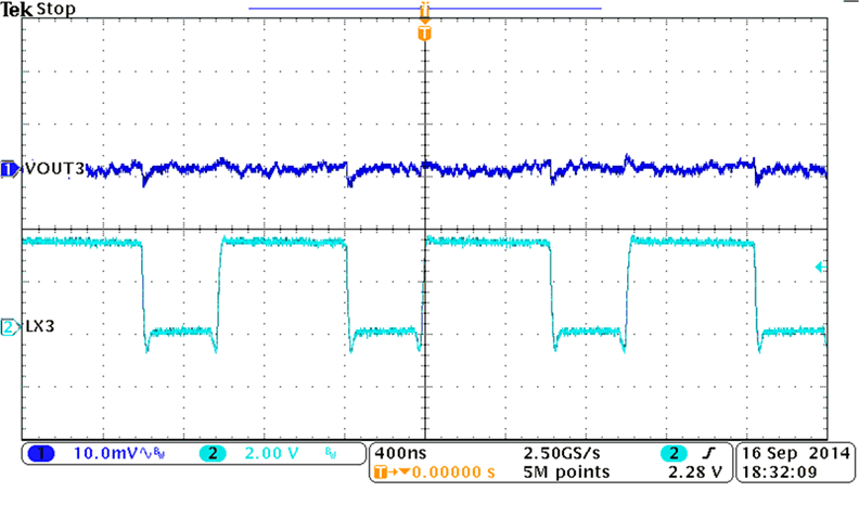
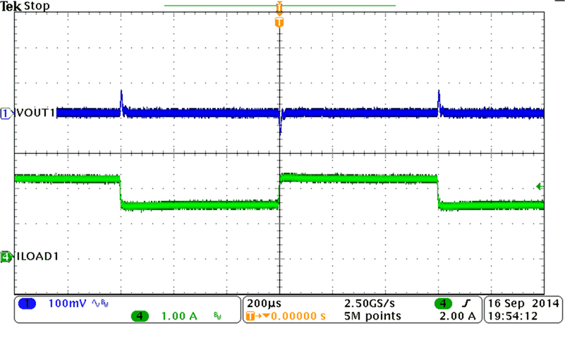
| SR = 0.25 A/µs | ||
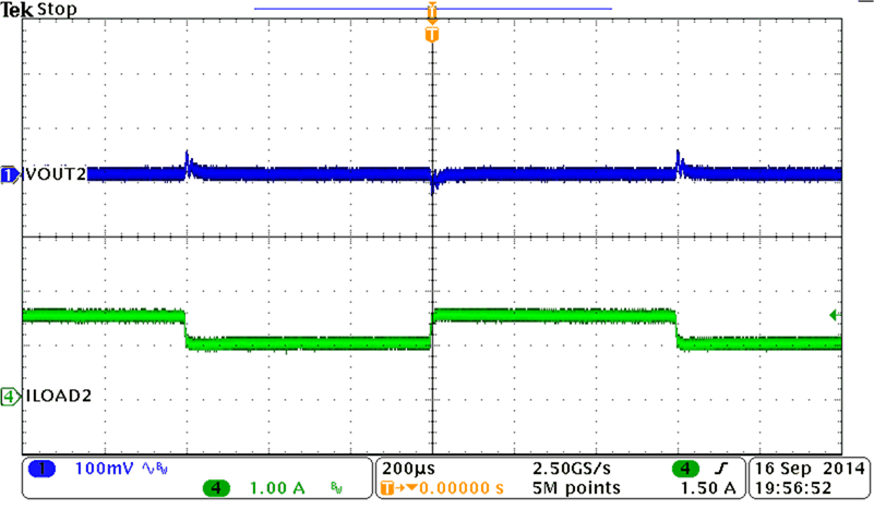
| SR = 0.25 A/µs | ||
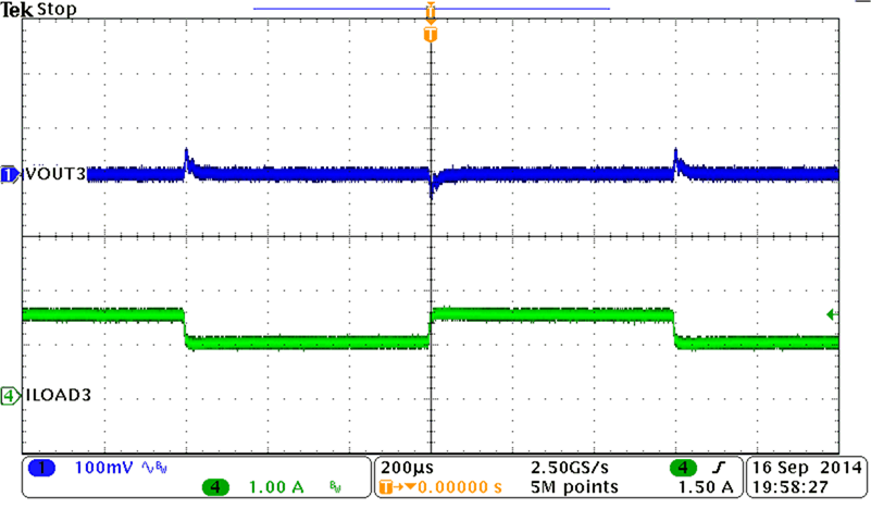
| SR = 0.25 A/µs | ||
