SLVSC85C August 2013 – May 2015 TPS65279
PRODUCTION DATA.
- 1 Features
- 2 Applications
- 3 Description
- 4 Revision History
- 5 Description (continued)
- 6 Pin Configuration and Functions
- 7 Specifications
-
8 Detailed Description
- 8.1 Overview
- 8.2 Functional Block Diagram
- 8.3
Feature Description
- 8.3.1 Enable and Adjusting Undervoltage Lockout (UVLO)
- 8.3.2 Adjustable Switching Frequency and Synchronization
- 8.3.3 Soft-Start Time
- 8.3.4 Out-of-Phase Operation
- 8.3.5 Output Overvoltage Protection (OVP)
- 8.3.6 Bootstrap Voltage (BOOT) and Low Dropout Operation
- 8.3.7 Overcurrent Protection
- 8.3.8 Current Sharing Operation
- 8.3.9 Thermal Shutdown
- 8.4 Device Functional Modes
- 9 Application and Implementation
- 10Power Supply Recommendations
- 11Layout
- 12Device and Documentation Support
- 13Mechanical, Packaging, and Orderable Information
Package Options
Mechanical Data (Package|Pins)
Thermal pad, mechanical data (Package|Pins)
Orderable Information
9 Application and Implementation
NOTE
Information in the following applications sections is not part of the TI component specification, and TI does not warrant its accuracy or completeness. TI’s customers are responsible for determining suitability of components for their purposes. Customers should validate and test their design implementation to confirm system functionality.
9.1 Application Information
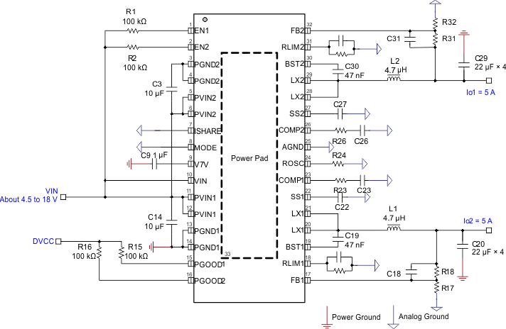
The devices are step-down DC-DC converters. They are typically used to convert a higher dc voltage to a lower dc voltage with a maximum available output current of 5/5 A. The following design procedure can be used to select component values for the TPS65279. Alternately, the WEBENCH® software may be used to generate a complete design. The WEBENCH software uses an iterative design procedure and accesses a comprehensive database of components when generating a design. This section presents a simplified discussion of the design process.
9.2 Typical Applications
9.2.1 Dual Buck Operation Mode Application
9.2.1.1 Design Requirements
For this design example, use the following in Table 1 as the input parameters.
Table 1. Design Parameters
| PARAMETER | EXAMPLE VALUE |
|---|---|
| Input voltage range | 4.5 to 18 V |
| Output voltage | 1.2 V/1.8 V |
| Transient response, 1.5-A load step | ΔVout = ±5% |
| Input ripple voltage | 400 mV |
| Output ripple voltage | 30 mV |
| Output current rating | 5 A |
| Operating frequency | 600 kHz |
9.2.1.2 Detailed Design Procedure
9.2.1.2.1 Adjusting the Output Voltage
The output voltage is set with a resistor divider from the output node (VOUT) to the FB pin. TI recommends to use 1% tolerance or better divider resistors.
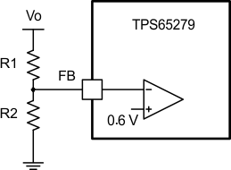 Figure 20. Voltage Divider Circuit

Start with a 40.2-kΩ for R1 and use Equation 3 to calculate R2. To improve efficiency at light loads consider using larger value resistors. If the values are too high, the regulator is more susceptible to noise and voltage errors from the FB input current are noticeable.
The minimum output voltage and maximum output voltage can be limited by the minimum on time of the high-side MOSFET and bootstrap voltage (BOOT-LX voltage) respectively. See Bootstrap Voltage (BOOT) and Low Dropout Operation for more information.
9.2.1.2.2 Adjusting UVLO
If an application requires either a higher UVLO threshold on the VIN pin or a secondary UVLO on the PVIN, in split rail applications, then the EN pin can be configured as shown in Figure 21.
When using the external UVLO function, TI recommends to set the hysteresis to >500 mV.
The EN pin has a small pullup current IP which sets the default state of the pin to enable when no external components are connected. The pullup current is also used to control the voltage hysteresis for the UVLO function since it increases by Ih once the EN pin crosses the enable threshold. The UVLO thresholds can be calculated using Equation 4 and Equation 5.
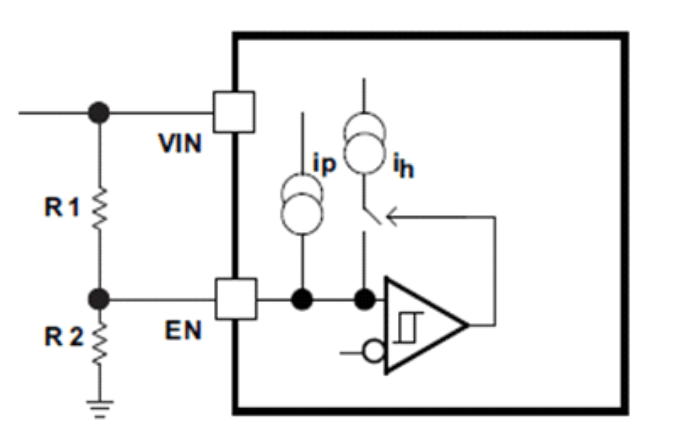 Figure 21. Adjustable VIN UVLO


where
- Ih = 3 µA
- IP = 3 µA
- VENRISING = 1.21 V
- VENFALLING = 1.17 V
9.2.1.2.3 Adjustable Switching Frequency (Resistor Mode)
To determine the ROSC resistance for a given switching frequency, use Equation 6 or the curve in Figure 22. To reduce the solution size one would set the switching frequency as high as possible, but tradeoffs of the supply efficiency and minimum controllable on time should be considered.
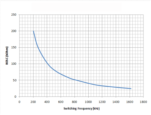 Figure 22. ROSC vs Switching Frequency

9.2.1.2.4 Output Inductor Selection
To calculate the value of the output inductor, use Equation 7. LIR is a coefficient that represents the amount of inductor ripple current relative to the maximum output current. The inductor ripple current is filtered by the output capacitor. Therefore, choosing high inductor ripple currents impact the selection of the output capacitor since the output capacitor must have a ripple current rating equal to or greater than the inductor ripple current. In general, the inductor ripple value is at the discretion of the designer; however, LIR is normally from 0.1 to 0.3 for the majority of applications.

For the output filter inductor, it is important that the RMS current and saturation current ratings not be exceeded. The RMS and peak inductor current can be found from Equation 9 and Equation 10.


The current flowing through the inductor is the inductor ripple current plus the output current. During power up, faults or transient load conditions, the inductor current can increase above the calculated peak inductor current level calculated above. In transient conditions, the inductor current can increase up to the switch current limit of the device. For this reason, the most conservative approach is to specify an inductor with a saturation current rating equal to or greater than the switch current limit rather than the peak inductor current.
9.2.1.2.5 Output Capacitor Selection
There are three primary considerations for selecting the value of the output capacitor. The output capacitor determines the modulator pole, the output voltage ripple, and how the regulator responds to a large change in load current. The output capacitance needs to be selected based on the most stringent of these three criteria.
The desired response to a large change in the load current is the first criteria. The output capacitor needs to supply the load with current when the regulator cannot. This situation would occur if there are desired hold-up times for the regulator where the output capacitor must hold the output voltage above a certain level for a specified amount of time after the input power is removed. The regulator is also temporarily not able to supply sufficient output current if there is a large, fast increase in the current needs of the load such as a transition from no load to full load. The regulator usually needs two or more clock cycles for the control loop to see the change in load current and output voltage and adjust the duty cycle to react to the change. The output capacitor must be sized to supply the extra current to the load until the control loop responds to the load change. The output capacitance must be large enough to supply the difference in current for 2 clock cycles while only allowing a tolerable amount of droop in the output voltage. Equation 11 shows the minimum output capacitance necessary to accomplish this.

where
- ΔIOUT is the change in output current.
- ƒSW is the regulators switching frequency.
- ΔVOUT is the allowable change in the output voltage.
For this example, the transient load response is specified as a 5% change in VOUT for a load step of 3 A. For this example, ΔIOUT = 3 A and ΔVOUT = 0.05 x 3.3 = 0.165 V. Using these numbers gives a minimum capacitance of 75.8 μF. This value does not take the ESR of the output capacitor into account in the output voltage change. For ceramic capacitors, the ESR is usually small enough to ignore in this calculation.
Equation 12 calculates the minimum output capacitance needed to meet the output voltage ripple specification.

where
- ƒSW is the switching frequency.
- Voripple is the maximum allowable output voltage ripple.
- Ioripple is the inductor ripple current.
Equation 13 calculates the maximum ESR an output capacitor can have to meet the output voltage ripple specification.

Additional capacitance deratings for aging, temperature, and DC bias should be factored in which increases this minimum value.
Capacitors generally have limits to the amount of ripple current they can handle without failing or producing excess heat. An output capacitor that can support the inductor ripple current must be specified. Some capacitor data sheets specify the root mean square (RMS) value of the maximum ripple current. Equation 14 can be used to calculate the RMS ripple current the output capacitor needs to support.

9.2.1.2.6 Input Capacitor Selection
The TPS65279 requires a high-quality ceramic, type X5R or X7R, input decoupling capacitor of at least 10-µF of effective capacitance on the PVIN input voltage pins. In some applications additional bulk capacitance may also be required for the PVIN input. The effective capacitance includes any DC bias effects. The voltage rating of the input capacitor must be greater than the maximum input voltage. The capacitor must also have a ripple current rating greater than the maximum input current ripple of the TPS65279. The input ripple current can be calculated using Equation 15.

The value of a ceramic capacitor varies significantly over temperature and the amount of DC bias applied to the capacitor. The capacitance variations due to temperature can be minimized by selecting a dielectric material that is stable over temperature. X5R and X7R ceramic dielectrics are usually selected for power regulator capacitors because they have a high capacitance to volume ratio and are fairly stable over temperature. The output capacitor must also be selected with the DC bias taken into account. The capacitance value of a capacitor decreases as the DC bias across a capacitor increases. For this example design, a ceramic capacitor with at least a 25-V voltage rating is required to support the maximum input voltage. TPS65279 may operate from a single supply. The input capacitance value determines the input ripple voltage of the regulator. The input voltage ripple can be calculated using Equation 16.

9.2.1.2.7 Loop Compensation
Integrated buck DC/DC converter in TPS65279 incorporates a peak current mode control scheme. The error amplifier is a transconductance amplifier with a gain of 1350 µA/V. A typical type II compensation circuit adequately delivers a phase margin between 60° and 90°. Cb adds a high frequency pole to attenuate high frequency noise when needed. To calculate the external compensation components, follow the following steps.
- Select switching frequency ƒsw that is appropriate for application depending on L and C sizes, output ripple, EMI, and etc. Switching frequency between 500 kHz to 1 MHz gives best trade off between performance and cost. To optimize efficiency, lower switching frequency is desired.
- Set up cross over frequency, ƒc, which is typically between 1/5 and 1/20 of ƒsw.
- RC can be determined by:
- gM is the error amplifier gain (1350 μA/V).
- gmps is the power stage voltage to current conversion gain (10 A/V).
- Calculate CC by placing a compensation zero at or before the dominant pole:
- Optional Cb can be used to cancel the zero from the ESR associated with CO.

where


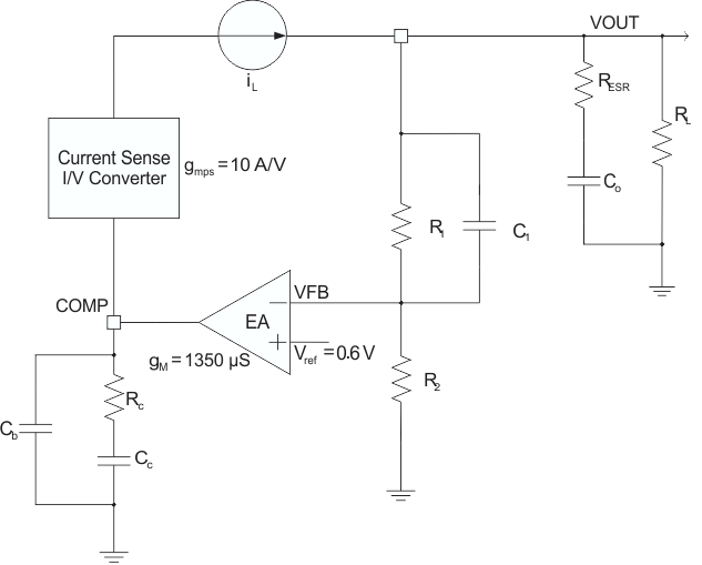 Figure 23. DC/DC Loop Compensation
9.2.1.3 Application Curves
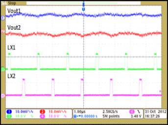
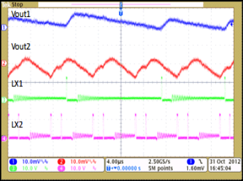
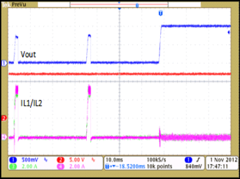
Buck2 at 0.2 A Auto PSM-PWM Mode
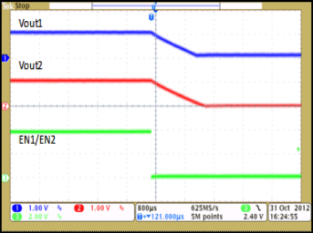
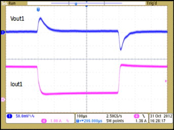
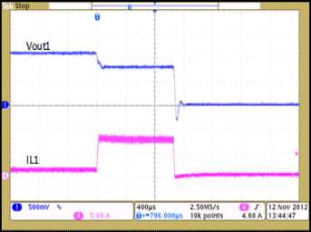
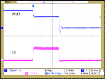
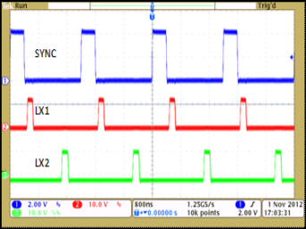
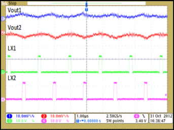
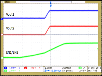
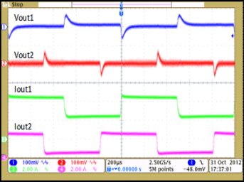
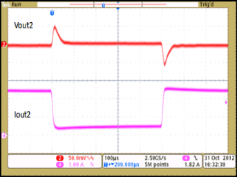
Buck2 0.5 A - 2.5 A
9.2.2 Current Sharing Mode Operation Application
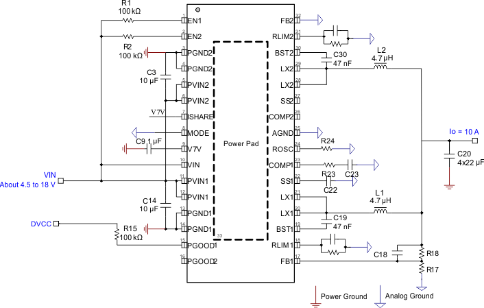 Figure 37. Share Mode Operation to Deliver 10 A
9.2.2.1 Design Requirements
See previous Design Requirements.
9.2.2.2 Detailed Design Procedure
As TPS65279 utilizes peak current mode control method, the two buck converters can be paralleled together to provide large current. The converters will work in current sharing mode by connecting the iShare pin to high. Once in current mode, signal pins in Buck 2 are not active, for example, FB2, COMP2, SS2, these pins will be neglected. Connecting FB2 to GND and floating COMP2, SS2, PGOOD2 are recommended.
For other component selection, refer to previous Detailed Design Procedure.
9.2.2.3 Application Curves
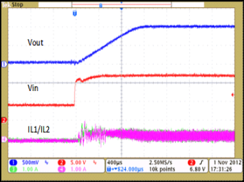
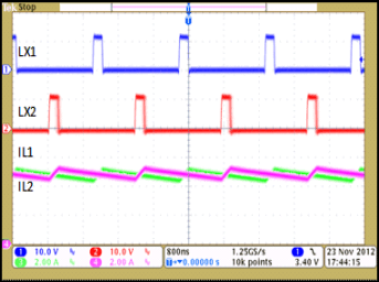
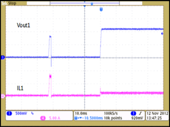
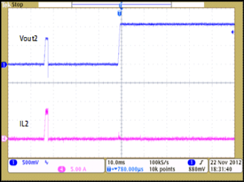
Current Share Mode Operation (IO = 10 A)
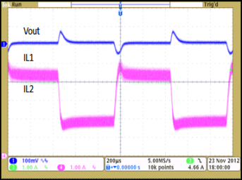
Current Share Mode Operation (IO = 4 A - 9 A)
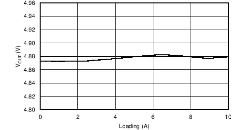
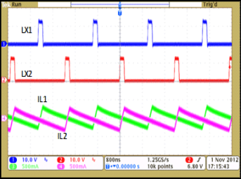
Current Share Mode Operation (IO = 0 A)
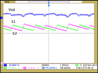
Current Share Mode Operation (IO = 10 A)
